Download
1 / 14
140 likes | 200 Views
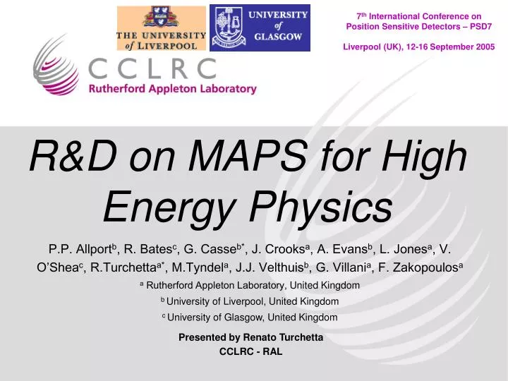
R&D on MAPS for High Energy Physics. P.P. Allport b , R. Bates c , G. Casse b* , J. Crooks a , A. Evans b , L. Jones a , V. O’Shea c , R.Turchetta a* , M.Tyndel a , J.J. Velthuis b , G. Villani a , F. Zakopoulos a a Rutherford Appleton Laboratory, United Kingdom

E N D
R&D on MAPS for High Energy Physics P.P. Allportb, R. Batesc, G. Casseb*, J. Crooksa, A. Evansb, L. Jonesa, V. O’Sheac, R.Turchettaa*, M.Tyndela, J.J. Velthuisb, G. Villania, F. Zakopoulosa a Rutherford Appleton Laboratory, United Kingdom b University of Liverpool, United Kingdom c University of Glasgow, United Kingdom
Outline Introduction. Monolithic Active Pixel Sensors (MAPS) aka CMOS sensors for imaging. Requirements Results Noise Radiation hardness CMOS sensors with in-pixel storage: Flexible APS (FAPS) Conclusions
CMOS Image Sensors akaMonolithic Active Pixel Sensor (MAPS) CMOS sensors for imaging, introduced in early ’90s. At the beginning, CMOS sensors used for low-end applications Constant improvement in the technology: noise, QE, … CMOS sensors widely used in high-end consumer and prosumer cameras For high-speed imaging (industrial, HDTV, …) CMOS sensors have already the best performance in terms of noise. All major players in imaging field are improving the technology. IEEE Workshop on CCD and Advanced Image Sensors IEEE Workshop on Image Sensors
Readout control Column-parallel ADCs Camera control Data processing / Output stage CMOS Monolithic Active Pixel Sensor • Standard CMOS technology • all-in-one detector-connection-readout = Monolithic • small size / greater integration • low power consumption • radiation resistance • system-level cost • Increased functionality • increased speed (column- or pixel- parallel processing) • random access (Region-of-Interest ROI readout) Camera-on-a-chip What is needed for Particle Physics ?
Potential barriers - + - + - + - + - + - + - + - + - + - + MAPS for particle detection Radiation • Requirements • Efficiency: 100% or close • Noise: signal ~ 100s e-/h pairs • Radiation hardness: Mrad and beyond • Speed: ‘frame rate’ > 106/sec • Large area: side ~ cm’s Metal layers Dielectric for insulation and passivation Polysilicon N+ N+ P+ N+ P-Well N-Well P-Well High energy particles generate about 80 e-/h pair per mm P-epitaxial layer P-substrate
RAL Sensors for Particle Physics UK collaboration to develop MAPS for Particle Physics and Space Science (also Leicester/Brunel, Birmingham) Parametric test sensor: RAL_HEPAPS family RAL_HEPAPS1: 0.25 mm, 2 mm (!) epitaxial layer, 64*8 pixels, 15 mm pitch: 3MOS, 4MOS RAL_HEPAPS2: 0.25 mm CIS, 8 mm epitaxial layer, 384*224 pixels, 15 mm pitch: 3MOS, 4MOS, ChargePreAmplifier (CPA), Flexible APS (FAPS, 20 mm pitch) RAL_HEPAPS3: 0.25 mm MM, no epitaxial layer, 192*192 pixels, 15 mm pitch: 3MOS, 4MOS, Deep N-well diodes Test sensors RAL_HEPAPS4: 0.35 mm CIS, 20 mm epitaxial layer, 1026*384 pixels, 15 mm pitch. 3 versions: 1, 2 or 4 diodes per pixel. Rad-hard, 5MHz row rate (manufactured, preparing tests)
Measured noise distributions for a 64x64 pixel test structure. Not corrected for system noise Soft reset RESET ~ Vreset. A factor of >~2 reduction (reset in the dark) Hard reset RESET – Vreset > Vth for reset transistor Noise (ENC in e- rms) Noise (ENC in e- rms) Soft and hard reset Vreset RESET ROW_SELECT Diode Output
Radiation hardness Transistors. Threshold shift: reduces with shrinking feature size Bird’s beak effect: use enclosed geometry transistors Transistor leakage current: use guard-rings to separate transistors Diodes. Radiation damage increases leakage current Radiation damage reduces minority carrier lifetime diffusion distance is reduced 0.25 micron ~tox2
No rad 1014 Device simulation. Single diode 15 mm pixel Device simulation. 4-diode 15 mm pixel No rad 1015 Single pixel S/N dependence on impact point • Less variation in S/N varies over pixel before and after irradiation. • S at edges still usable after 1015 p/cm2. G. Villani (RAL)
Landau Distributions Beta source (Ru106) test results. Sensors HEPAPS2. Examples of clusters. S/N per pixel Landau distributions Summary table
Noise (ADU counts) S/N Dose (log10(p/cm2)) Signal (ADU counts) Dose (log10(p/cm2)) Dose (log10(p/cm2)) Radiation test. Summary • Sensors yield reasonable S/N up to 1014 p/cm2 • 0.35 mm technology in the pixel transistors. Enclosed layout in 3MOS_E • S/N reduction seems to be dominated by charge collection J. Velthuis (Liv)
Amplitude Light pulse Time Flexible Active Pixel Sensor Pulses LED test (single pixel) 10 memory cell per pixel 28 transistors per pixel 20 mm pitch 40x40 arrays Design for the Vertex detector at the International Linear Collider
Seed 3x3 5x5 FAPS. Landau distribution • Test with source • Correlated Double Sampling readout (subtract Scell 1) • Correct remaining common mode and pedestal • Calculate random noise • Sigma of pedestal and common mode corrected output • Cluster definition • Signal >8 seed • Signal >2 next • Note hit in cell i also present in cell i+1. • S/Ncell between 14.7±0.4 and 17.0±0.3 J. Velthuis (Liv)
Conclusions Parametric test sensors used to study noise, radiation hardness, new designs. Radiation hardness 1014 p/cm2 Noise < 20 e- rms (soft reset in dark) Three versions for radiation hardness of fast (5MHz/line), rad-hard, large (1024*384) sensor (RAL_HEPAPS4) manufactured FAPS architecture developed for vertex detector at ILC Digital pixel architecture (R&D within MI3 collaboration, N. Allinson et al.) in development for CALICE Electromagnetic Calorimeter at ILC (P. Dauncey, Imperial College et al.). Would require large area coverage 104 m2, stitched sensors CMOS technology could provide the solution for coverage of large areas with pixel detectors