Download
1 / 73
740 likes | 1.1k Views
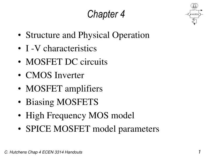
Structure and Physical Operation I -V characteristics MOSFET DC circuits CMOS Inverter MOSFET amplifiers Biasing MOSFETS High Frequency MOS model SPICE MOSFET model parameters. Chapter 4. MOSFET ID-VG, ID-VDS. Output Charc. Input Charc.

E N D
Structure and Physical Operation I -V characteristics MOSFET DC circuits CMOS Inverter MOSFET amplifiers Biasing MOSFETS High Frequency MOS model SPICE MOSFET model parameters Chapter 4
MOSFET ID-VG, ID-VDS Output Charc. Input Charc. IDsat = n Cox W/L (VGS - VTN)2/2 --- SQUARE LAW L>250nm Subthreshold Leakage
MOSFET ID-VG, ID-VDS Output Charc. Input Charc. IDsat = vsat Cox W K (VGS - VTN) “Linear” L<250nm VTN Subthreshold Leakage
MOSFET ID-VG, ID-VDS Digital Logic Analog VTN VDD = 1
Anatomy of an Inverter PMOS NMOS PMOS Oxide NMOS
MOS Transistor Operating Regions VDD VDD
Triode or Linear Region OFF VGS < VT or VTO
Triode or Linear Region TRIODE VDS < VGS -VT
Cgs ON/Triode: V > 0 or VGS > VTO Cgs = WL Cox; V > VDS OFF: V < 0 or VGS < VTO Cgs WL Cox Sat: V < 0 or VGS < VTO Cgs = 2/3 WL Cox ; V < VDS NMOS N Diffusion PMOS P Diffusion PolySilicon
SPICE MODEL parameters Over 200 parameters define Modern 65nm MOSFETs 2000nm V = VGS-VT0 KP = Uo Cox
ID vs. VGS; VDS > V L > 250nm Square Law L < 250nm Vel. Sat.
ID vs. VGS; VDS > V Supplemental Taking the square root of ID and solving for slope & intercept; Extract VTO and KP
Enhancement/ Depletion Mode NMOS – 1st Quadrant PMOS – 3rd Quadrant Enhancement VTN > 0V VTP < 0V Depletion Mode VTN > 0V VTP < 0V
MOSFET parameters Ex -graphical ; V < VDS ID= W/LnCox (VGS - VTN)2/2 --- Sat. n Cox W/L = ID = W/L n Cox {V VDS + VDS2/2}---Triode or Lin Region
CMOS Inverter – Strong pull up & down Rise time Fall Time
INVERTER POWER Supplemental
Why CMOS Inverter NMOS PMOS
CMOS Logic NMOS pull dwn Zbar = AB+CD
CMOS Logic PMOS pull UP Z = A’+B’ C’+D’
CMOS Logic PMOS pull UP Z = A’+B’ C’+D’
CMOS Logic PMOS pull UP Z = A’+B’ C’+D’ Supplemental
CMOS Logic Supplemental
CMOS Logic & Scaling If CL 3 minimum loads or 7.5fF 0.5um process OR 1.25fF 90nm process Note tr & tf NOT equal?
CMOS Logic & Scaling > 6-7X less Pwr
CMOS Logic NMOS pull DWN Z’ = A(D+E) + (BC) PMOS pull UP Z = [A+(D E)] (B+C) PMOS pull UP Z = A’+B’ + C Supplemental NMOS pull DWN Z’ = ABC
Shifting the Qpt for Gain A Gain A = ΔVDS/ ΔVGS
CMOS Analog ID vs. VDS & rds Early Voltage and Lambda Take Away – effective output resistance Modeled by 1/ID or VA/ID
Developing the Bias Current • Setting biasing Current of Diff Amp, Note: • I R = ID6 • VDD -VSS= VSG + IB RB; R = (ß·2VDD - VTN) - (2·I))/(I·ß)
Diff Amp Current Behavior Starting Eq 1 & 2 Solving 1 & 2
Diff Amp Testing Case 1 Vin = 0, Io = 0 Case 2 -2xV < Vin < +2xV Case 3 Vin > | 2xV|; Io = IB
ID vs. VGS - ID vs. VDS; Amplification & gm
ID vs. VGS - ID vs. VDS; Amplification
Q pt Bias Stabilization Amplification
f1 Bias Considerations (Hi Pass) Amplification
f1 Bias Considerations(Hi Pass) Amplification
f2 Considerations(low pass) Amplification
Common Source Summary • Select Qpt = (VGS, ID, & VDS)and estimate gm and gds =ID/VA • Stabilize the Bias or Quiescent point – VGG =VGSQ + ID RS • RG1, RG2 and RS = VGSQ/IDQ VGG =VDD RG1/{RG1|| RG2} • Determine Cc1, Cc2, CS • Determine RD after finding gm and gds. • gain = -gm RD||rds||RL mid band gain • Generally – RL >> RD or rds & RG = RG||RG >> Rgen
Common Source Summary``
Biasing Example; GIVEN – Beta = 50mA/V, VT=0.7 & VA = 5, CISS = 1 pF Qpt is to be VGS = 1.0V, ID = 2.25mA, VGS /ID = 400
Biasing Example; GIVEN – Beta = 50mA/V, VT=0.7 & VA = 5, CISS = 1 pF Qpt is to be VGS = 1.0V, ID = 2.25mA, VGS /ID = 400