Download
1 / 35
350 likes | 464 Views
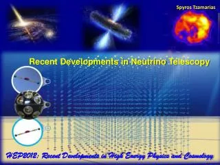
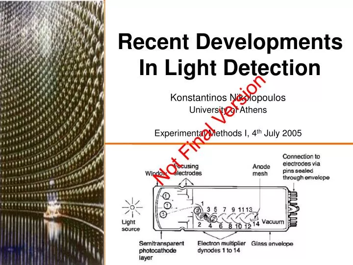
Recent Developments In Light Detection. Konstantinos Nikolopoulos University of Athens Experimental Methods I, 4 th July 2005. Not Final Version. Pierre Auger Prototype Fluorescence telescope camera (440 photomultiplier tubes). Super – Kamiokande 20- inch PMT tube (Venetian Blind).

E N D
Recent Developments In Light Detection Konstantinos Nikolopoulos University of Athens Experimental Methods I, 4th July 2005 Not Final Version
Pierre Auger Prototype Fluorescence telescope camera (440 photomultiplier tubes) Super – Kamiokande 20- inch PMT tube (Venetian Blind) Why detect light? Usage of Light detection in High Energy Physics* *short list of indicative examples Light is used in many aspects of HEP experiments • Calorimetry • Tracking • Scintillating Fiber Trackers • Particle Identification • Cherenkov • Medical Imaging • PET • SPECT Light Detectors are used in enormous numbers at HEP • Super – Kamiokande • Cherenkov Counters 13.000 PMTs • Pierre Auger Observatory • Fluoresence Detectors 10.560 PMTs Light detection is crucial for every kind of high energy physics experiment. Aim of this presentation is summarize current trends in light detection
Physics of Light Detection • Photoelectric Effect • When a photon impinges on the surface of any material, it can liberate an electron provided that the photon energy is higher than the photoelectric workfunction Φ. The liberated electron carries kinetic energy W=hν-Φ, which can be sufficient to bring the electron not only from the surface, but also from the volume of the material to the free space. • Semiconductors have a very small workfunction Φ. • Electron lift from Valence Band to Conduction Band in a Semiconductor • When an photon impinges on a semiconductor, then an electron from the valance band can be lifted to the conduction band. When the electron cannot recombine with the hole, due to the electric field of a silicon photodiode, it can be collected and the signal amplified. The second process is far more efficient in light detection both in terms of detection efficiency and wavelength sensitivity, because it needs less energy O(1 eV) than the photoelectric effect one O(10 eV).
Main Characteristics of Light Detectors • Quantum Efficiency • The efficiency in single photon detection • Gain • Multiplication of the initial signal • Sensitivity • Minimum # of photons required for output signal • High – Voltage Supply • Timing and Positioning • Capability of providing time and position information of the incoming photon • Noise • Dark current • Nuclear counter effect (=The extra amount of charge produced in the photodiode by a charged particle directly hitting it, on the top of the charge produced by th scintillation light). • Experimental Conditions • B-field, Temperature, Radiation Levels, Particle Rate, e.t.c. • Complexity of construction • Physical Shapes of Detectors • Price
Types of Light Detectors • Vacuum Devices • Solid – State Devices • Hybrid Devices • Gaseous Detectors
Vacuum Devices Features: • Low noise amplification • Due to the dynode – chain amplification scheme. Only noise contribution is the stochastic nature of the secondary e- emission • High Gain O(106) • Output read by standard electronics No need for amplification No additional noise • Gain = f(# dynodes) • Good Energy resolution • Calorimeters with scintillating crystals • Single photon detection The first photoelectric tube was produced by Elster and Geiter in 1913. The first photomultiplier tube was invented by the RCA laboratories in 1936.
Box – and – grid Circular Cage Linear Focused Venetian Blind Vacuum Devices II Many dynode chain design exists, with different properties! • Linear Focused Type • Fast Response • Linearity • Large Output Current • Box - and - Grid Type • Consist of a series of quarter cylindrical dynodes. • Electron collection efficiency • Uniformity • Circular Cage Type • Compactness • Fast Response • High gain (with relatively low High—Voltage) • Venetian Blind Type • Large dynode area (large photocathode area) • Uniformity • Large Output current
Vacuum Devices III Drawbacks: • Q.E. typically constrained to ≈25% • Reflection of photons by the glass of the window • Passage of photons through the photocathode without interaction • The produced photoelectrons may stop inside the cathode material • Shape dictated by technical restrictions in the fabrication of the vacuum container • Hand work involved Expensive to construct • Very sensitive to B – field • Defocusing of the e-
Metal – Channel Device Mesh Dynodes Further Innovations in Vacuum Devices • Sensitivity to B—field • Dynodes from meshes with small distance O(1mm) and high field between them. • Information on the position of the incoming photons • Metal – channel devices. The single dynode chain is replaced by many chains in parallel and there is a segmented anode. • New photocathode and window materials
Solid – State Devices Photosensors made of semiconductor material gained much attention in recent years. • High Q.E. • Main negative contribution is the reflection at the surface • Insensitivity to magnetic fields • Theoretical Limit ≈ 15 T • Produced in standard fully – automated processes • Inexpensive • Fairly easy to be tailored for individual needs • In short time • Low mass • Small space consumption • Thickness < 1/2 mm They open new areas of application!
PIN Photodiode • The PIN photodiode is a semiconductor device, typically fabricated using doped silicon. In a photodiode, absorption of an incoming photon produces a single electron-hole pair. A small electric field within the photodiode causes these charge carriers to migrate in opposite directions towards external electrodes. This results in a measurable current or voltage, which has a linear relationship to the incident light flux. • The silicon PIN diode is a very successful device. All major experiments in high-energy physics used it in big numbers in the last 2 decades. The operation is simple and reliable but since it has no gain it needs a charge-sensitive amplifier that adds to the cost and creates noise in the readout system. Single photon detection with silicon photodiodes is therefore not possible and the very good timing properties (1–2 ns) are destroyed by the signal rise time of the amplifier which is 10 ns or more. • Arrays of photodiodes are easy to produce and are commercially available
Schematic Diagram of an APD Hamamatsu S8148 Avalanche Photodiodes • Avalanche Photodiodes provide gain due to the high internal field at the junction of positively and negatively doped silicon. • The incoming photon produces an e-h pair. • The electron gain enough energy due to the high internal field to produce secondary electrons by impact ionization • An electron avalanche is created • Gain is 50 – 200. • Higher gains (up to 104) can achieved • Q.E. is of O(80%). • Large Dynamic range • Excellent energy resolution • Position information • Only with dedicated setup position resolution O(0.3mm) • Drawback: Very stable environment of operation needed for gains over a few hundreds. • 1% gain variation δT= 0.1 K or δV/V=10-4
Avalanche Photodiodes in Geiger Mode • In this case the APD is operated at a bias voltage higher than the breakdown voltage. • Any photon or thermally liberated electron starts an avalanche. • The avalanche persists until the voltage is lowered actively or when the voltage drops on a properly chosen serial resistance. • The output signal is proportional to the over – voltage and the capacitance of the APD. • Drawback: There is a long dead time O(1 ms) after each breakdown.
Silicon Photomultipliers (SiPM) • The SiPM is a novel type of APD. • It is a multipixel silicon photodiode with a number of micropixels of size O(20 μm) joined together on common substrate and working on common load. • The operational bias voltage is ≈15% higher than the breakdown voltage. • The pixels are electrically decoupled from each other. • Each SiPM pixel operates in Geiger mode • Each SiPM pixel operates as a binary device • The SiPM as a whole is an analogue detector. The SiPM intend to solve the problem of long dead time in the APDs functioning in Geiger mode.
Single Photon Detection Efficiency of a SiPM, a APD and a classical PMT Silicon Photomultipliers II • Detection efficiency. • Q.E. is of O(80%). • εgeometrical=Ssensitive/Stotal, is of O(25%). • Gain O(106) • Independent of primary carrier number. • Excellent energy resolution. • Dynamic range O(10^3/mm^2). • <#photons/pixel> << 1 (signal saturation) • Electronics noise is negligibly small • High gain • Electronic noise contribution < 0.1 e- • Main noise contribution is the dark rate. • Originates from carriers created thermally in sensitive volume or due to effects of high electric fields. • O(1 MHz/mm2) @ room temperature • ≈1kHz/mm2 @ 100 K • However, dark rate limits SiPM performance only in detection of very small light intensities O(1 ph.e.).
Response of SiPM to light of very low intensity. The number of photons can be counted for each event. Silicon Photomultipliers (SiPM) III • Insensitive to B – fields • Excellent time resolution (≈100 ns) for single photo – electron detection • Time Resolution obeys the Poissonian law of 1/√Npixelsfired • Fast rise time ≈1ns • The discharge is contained within a limited region in the depletion zone (due to the voltage distribution) small duration • Does not suffer from nuclear counter effects • Stable operation in room temperature • Low gain variation with temperature • ΔΤ = 2.5 Κ for 1% gain variation. • Does not exhibit any serious radiation damage • Perhaps Neutrons are an exception to this rule
Simulated potential distribution and electron trajectory Schematic view of the Pixel HPD Hybrid Detectors (HPD) • These detectors combine the advantages of the vacuum devices and the solid – state devices • Pixel – HPD • Pad – HPD • The vacuum container and the photocathode are the same as in the classical PMT. • The photo – electrons are accelerated in a high electric field and are focused onto an anode: • A silicon PIN photodiode, an amplification of 4000 is achieved with an electric field of 15kV. • An APD, a gain of more than 105 can be achieved, allowing usage of simple readout electronic circuit.
Typical photoelectron spectrum Hybrid Detectors (HPD) II • Q.E. is of O(20%) @ 270 – 400 nm • εgeometrical is of O(80%). • Using electron optics. • Position information • When the anode is segmented. • The HPDs have a very good energy resolution, even for light of very low intensity.
Electric Field profile in a VLPC Schematic Layout of a VLPC Visible Light Photon Counters (VLPC) VLPCs are solid state photo – detectors, originally invented at Rockwell International and presently developed and manufactured by Boeing. • The operation principle of VLPCs is the effect of impurity band. • Occurs when a semiconductor is heavily doped with shallow donors or acceptors. • The impurity atoms are close together electrical transport occuring by charge hopping from impurity site to impurity site! • The standard 1.12 eV gap of Si is used to absorb photons • The small gap with the impurity band is used for creating an electron – D+ avalanche multiplication. • Small gap O(0.05eV) Relatively low field is required for avalanche the required field for producing an avalanche is low. • Localized and self– limiting avalanche(due to local field collapse, D+ have low mobility) • The drift region can been seen as an internal resistor in series with an ideal VLPC
VLPC Single Photoelectron counting capabilities Visible Light Photon Counters II • High Q.E. (80%). • High gain O(5* 10^4). • Low gain dispersion. • Operational in a high background radiation enviroment. • Drawback: Cryogenic temperatures needed! • In order to freeze out the intrinsic carriers!
Gaseous Detectors • These detectors have been developed for cases that large areas are needed to be covered. • Their functionality principle relies on photo – conversion and subsequent multiplication in a gas avalanche. • The photo--conversion can be in the gas itself or in a CsI photocathode, which can be made in large areas. • Readout: MWPC e.t.c.
Field Distribution in the Gas – Electron Multiplier foil Gaseous Detectors II • Main problem: Ion and photon feedback • Ion Feedback, ionization of the residual gas (Vacuum) or the gas used (gaseous detectors) in the detector. Collision of the gas molecules with electrons can cause the ionization of the gas then a pulse can be created • Positive ions striking the front dynodes or the photocathode may produce many secondary electrons large noise pulse • This new pulse usually follows a true photo –electric pulse after pulsing • Solved to some extent by “the gas electron multiplier (GEM) foil” technique
The ATLAS detector ATLAS Tile Calorimeter Schematic Layout The ATLAS Tile Calorimeter • ATorodial LHC ApparatuS is general purpose detector to study proton – proton collisions @ √s=14 TeV (some Heavy – Ions Program is foreseen as well) • ATLAS is mostly known for its Muon System, however as a general purpose apparatus, ATLAS should be able to perform accurate calorimetry as well. • The ATLAS calorimetry system is quite complicated, incorporating different approaches • Liquid Argon Sampling Electromagnetic Calorimeter |η|<3.2 • Liquid Argon Hadronic Calorimeter 1.5<|η|<3.2 • Tile Hadronic Calorimeter |η|<1.7 • Forward Calorimeter 3.2<|n|<4.9 (Liquid Argon)
Tile Calorimeter: Operation Principle ATLAS polysterene tiles The ATLAS Tile Calorimeter II • Tile Calorimeter • Active medium: Tiles of polysterene (emission maximum ≈100 nm) • Absorber :Steel • Wavelength Shifter Fibers (≈100nm ≈400nm) • Photo – Multiplier Tubes (10.500) (max sensitivity ≈420nm) • PMT characteristics • Min/Max wavelength = 300nm/650nm • Max sensitivity @ 420nm • Window : Borosilicate • Photocathode : Bialkali • Gain = 3 105 • Dark Current = 2 nA • Rise Time = 1.5 ns • Transit Time = 7 ns • Transit Time Spread = 0.26 ns • Number of dynodes = 8 • Operation Voltage = 800 Volt
The KLOE Electromagnetic Calorimeter The main aim of KLOE is to do high precision CP – Violation studies in K0 decays a the Frascati Φ– Factory DAFNE. The Electromagnetic Calorimeter Sampling calorimeter: Scintillating Fibers are glued inside thin grooved lead layers. Volume ratio of the composite Pb:scint:glue of 42:48:10 and X0=1.5 cm. Total depth is 23 cm (15 X0) . Containment: 98% of 500 MeV e/m showers (Maximum shower energy at KLOE). Scintillating fibers Excellent time resolution for long detectors. Relatively long attenuation lenght Total fiberslenght is 15000 Km! PMTs with Mesh dynodes are used E/M Calorimeter inside B-field. B- filed strength ≈0.1-0.2 T at the readout. The total number of PMTs is 4880. π0mass reconstruction using KLOE’s calorimeter KLOE Electromagnetic Calorimeter
The PbW04 scintillating crystals used by CMS ECal Energy Resolution measured with 180 GeV electrons in 3x3 crystal matrix with 2 APDs/crystal readout Schematic layout of the CMS ECAL The CMS apparatus The CMS Electromagnetic Calorimeter • CMS is a general purpose detector for the Large Hadron Collider • CMS Electromagnetic Calorimeter • Homogenous calorimeter • 75.000 PbW04 scintillating crystals used. • Calorimeter dimensions: Longitudinal 25 X0 = 22.2 cm Transverse 1 RM = 2.2 cm • Operation in high B-field 4T • Very High radiation leves • One APD mounted on each side of the crystal depth of interaction.(Sufficient pulse height from the APDs) • Many sources to be kept under control: • Longitudinal uniformity of light collection • Strong light yield variation with temperature (-2.3%/0C) • APD gain variation with applied tension (-3%/Volt) and termperature (-2.3%/0C) • Light collection uniformity • light transmission due to radiation damage • Leakage front and rear
Cherenkov rings produced by 120 GeV π-, radiator C4F10 .The circle is guide to the eye. Typical Event from RICH1 Schematic Layout of RICH1 LCHb Schematic Layout LHCb Ring Imaging Cherenkov • LHCb is a single arm forward spectrometer designed to perform various B – physics measurements in the LHC. • 2 Ring Imaging Cherenkovs • RICH 1 Aerogel n =1.03 ( 2 – 10 GeV) C4F10 n =1.0014 (10 – 60 GeV) • RICH 2 CF4 n =1.0005 (16 – 100 GeV) • HPDs 61 pixel/HPD • Magnetic Field, High Radiation Dose
Schematic view of the D0 apparatus VLPC wafer The D0 SciFi Tracker • D0 is a general purpose apparatus to study √s=2 TeV proton – antiproton collisions at Tevatron. • Central Scintillating Fiber Tracker • Consists of 74.000 multi – clad scintillating fibers • refraction index 1.591.491.42 for improvement of light trapping • VLPCs • Q.E. 70%, • Gain 20.000 • Rate capability > 10 MHz • Noise Rate <0.1 % • Impurity band 0.05 below the conduction band • Operation at 9K
Layout of the GlueX apparatus The GlueX Barrel Electromagnetic Calorimeter • The goal of the GlueX experiment at Jefferson Laboratory is to search for gluonic excitations manifested in exotic hybrid vector mesons with masses up to 2.5 GeV, using linearly polarized photons of 8 – 10 GeV energy. • Electromagnetic Barrel Calorimeter • Sampling calorimeter • Scintillating fiber
Conclusions (continued) As concluding remarks we would like to focus on the following: • Light detection is crucial for every kind of High Energy Physics experiment. • One should also note that we didn’t mention at all a very closely related topic, that of light detection for medical purposes (PET e.t.c.). • The progress in the field of light detection is enormous. Today, the market offers light detectors for almost every need and funding. • Semiconductor devices are a very promising development in the field. It is expected to be further improved. • Further progress in the field can be expected.
References General • D. Renker, Photosensors, Nucl. Instr. And Meth. A 527 (2004), p.15 • Hamamatsu Photonics , http://www.hamamatsu.com/ Vacuum Devices • Hamamatsu Photonics, Photomultiplier Tubes (PMTs) – Construction andOperating Characteristics, http://www.hpk.co.jp/ APDs • I. Britvitch et al., Avalanche photodiodes now and possible developments, Nucl. Instr. And Meth. A 535 (2004), p.523 SiPM HPD E. Albrecht et al., Nucl. Instr. And Meth. A 442 (2000), p.164 L. Somerville, Pixel hybrid photon detectors for the ring imaging Cherenkov, Nucl. Instr. And Meth. A 546 (2005), p.81 A. Braem et al., Nucl. Instr. And Meth. A 504 (2003), p.19 VLPCs • M.D. Petroff, et al., Appl. Phys. Lett. 51 (1987) p. 406 A. Bross et al., Nucl. Instr. And Meth. A 477 (2002), p.172 Gaseous Experiments • The ATLAS experiment, http://atlas.web.cern.ch/Atlas/ • The CMS experiment, http://cmsinfo.cern.ch/Welcome.html/ • The LHCb experiment, http://lhcb.web.cern.ch/lhcb/ • The KLOE experiment, http://www.lnf.infn.it/kloe/ • The D0 experiment, http://www-d0.fnal.gov/ • The GlueX experiment, http://www.gluex.org/ • The Pierre Auger Obervatory, http://www.auger.org/ • Super-Kamiokande, US Collaboration homepage, http://neutrino.phys.washington.edu/~superk/
Schematic of a PET scanner Positron Emission Tomography • PET produces images of the body by detecting the radiation emitted from radioactive substances. These substances are injected into the body, and are usually tagged with a radioactive atom, such as (C-11, F-18, O-15, or N-13), that has a short decay time. (bombardment of normal chemicals with neutrons) • PET detects the gamma rays given off at the site where a positron emitted from the radioactive substance collides with an electron in the tissue. • PET provides images of blood flow or other biochemical functions, depending upon the type of molecule that is radioactively tagged. For example, PET can show images of glucose metabolism in the brain, or rapid changes in activity in various areas of the body. However, there are few PET centers in the country because they must be located near a particle accelerator device that produces the short-lived radioisotopes used in the technique.
Single Photon Emission Computed Tomography • Single Photon Emission Computed Tomography (SPECT)SPECT is a technique similar to PET. • The radioactive substances (Xenon-133, Technetium-99, Iodine-123) have longer decay times than those used in PET • Single photon emittance instead of double gamma rays. • SPECT can provide information about blood flow and the distribution of radioactive substances in the body. • Its images have less sensitivity and are less detailed than PET images. • SPECT technique is less expensive than PET. • SPECT centers are more accessible than PET centers because they do not have to be located near a particle accelerator.