Download
1 / 1
10 likes | 130 Views
Free Space Optical Communication Integrated Circuit (IC) Design. 2012. Printed Circuit Board (PCB ). Project Goal.

E N D
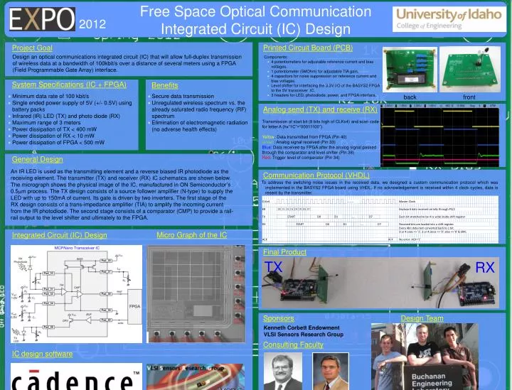
Free Space Optical Communication Integrated Circuit (IC) Design 2012 Printed Circuit Board (PCB) Project Goal Design an optical communications integrated circuit (IC) that will allow full-duplex transmission of wireless data at a bandwidth of 100kbit/s over a distance of several meters using a FPGA (Field Programmable Gate Array) interface. Components: • 4 potentiometers for adjustable reference current and bias voltages, • 1 potentiometer (5MOhm) for adjustable TIA gain, • 4 capacitors for noise suppression on reference current and bias voltages, • Level shifter for interfacing the 3.3V I/O of the BASYS2 FPGA to the 5V transceiver IC, • 3 headers for LED, photodiode, power, and FPGA interface. System Specifications (IC + FPGA) Benefits • Minimum data rate of 100 kbit/s • Single ended power supply of 5V (+/- 0.5V) using battery packs • Infrared (IR) LED (TX) and photo diode (RX) • Maximum range of 3 meters • Power dissipation of TX < 400 mW • Power dissipation of RX < 10 mW • Power dissipation of FPGA < 500 mW • Secure data transmission • Unregulated wireless spectrum vs. the already saturated radio frequency (RF) spectrum • Elimination of electromagnetic radiation (no adverse health effects) front back Analog send (TX) and receive (RX) Transmission of start bit (8 bits high of CLKx4) and scan code for letter A (hx“1C”=“00011100”) Yellow: Data transmitted from FPGA (Pin 40) Green: Analog signal received (Pin 33) Blue: Data received by FPGA after the analog signal passed through the comparator and level shifter (Pin 38) Red: Trigger level of comparator (Pin 34) General Design An IR LED is used as the transmitting element and a reverse biased IR photodiode as the receiving element. The transmitter (TX) and receiver (RX) IC schematics are shown below. The micrograph shows the physical image of the IC, manufactured in ON Semiconductor’s 0.5mm process. The TX design consists of a source follower amplifier (N-type) to supply the LED with up to 150mA of current. Its gate is driven by two inverters. The first stage of the RX design consists of a trans-impedance amplifier (TIA) to amplify the incoming current from the IR photodiode. The second stage consists of a comparator (CMP) to provide a rail-rail output to the level shifter and ultimately to the FPGA. Communication Protocol (VHDL) To address the switching noise issues in the received data, we designed a custom communication protocol which was implemented in the BASYS2 FPGA board using VHDL. If no acknowledgement is received within 4 clock cycles, data is resent by the transmitter. Micro Graph of the IC Integrated Circuit (IC) Design Final Product TX RX Design Team Sponsors Kenneth Corbett Endowment VLSI Sensors Research Group Consulting Faculty IC design software Dr. Suat Ay Dr. Ken Noren Pin-Jen Wang Markus Geiger Chris Goodale