Download
1 / 56
560 likes | 749 Views
ME 6405 Student Lecture: Transistors. Ryan Akin Xin Chen Will Dahlin. Thursday October 6, 2011 Georgia Institute of Technology. Presentation Outline. 1. Introduction to Transistors Ryan Akin. 2. Transistor Types and Checks Ryan Akin. 3. Bipolar Junction Transistors Xin Chen. 4.

E N D
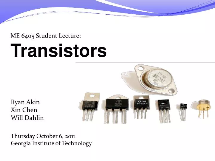
ME 6405 Student Lecture:Transistors Ryan AkinXin Chen • Will Dahlin Thursday October 6, 2011Georgia Institute of Technology
Presentation Outline 1 Introduction to Transistors Ryan Akin 2 Transistor Types and Checks Ryan Akin 3 Bipolar Junction Transistors Xin Chen 4 Field Effect and Power Transistors Will Dahlin 5 Transistor Part Numbers and Catalog Will Dahlin
Definition & Fundamental Need • Brief History • Transistor Role in Modern Electronics • Two Basic Transistor Functions • Doping process and its effects on function Introduction to Transistors
Transistors BJT (PNP) Electrical Diagram Representation Transistors of various type & size First Transistor Model, 1947 Used in all modern electronics FET Transistor BJT Transistor
tran·sis·tor • a semiconductor device that amplifies, oscillates, or switches the flow of current between two terminals by varying the current or voltage between one of the terminals and a third. (www.dictionary.com) www.coltecnica.com
Basic Purpose • [1] To electronically switch (no moving parts) a signal on or off (high/low) • [2] To amplify signals • Role in Modern Electronics • Basic building blocks for all modern electronics • Microprocessors, Microcontrollers, Computers, Digital watches, Digital Logic Circuits, Cell Phones…. Motor Controllers Microprocessor PC & Cell Phones Headphones
Reason for Transistor’s Invention: • Early 20th century, vacuum tube were used as signal amplifiers & switches. • Use of vacuum tube* resulted in extremely large, fragile, energy inefficient, and expensive electronics. • Evolution of electronics required device that was small, light weight, robust, reliable, cheap to manufacture, energy efficient… • *Vacuum tube advantages: operation at higher voltages (10K region vs. 1K region of transistors); high power, high frequency operation (over-the-air TV broadcasting) better suited for vacuum tubes; and silicon transistors more vulnerable to electromagnetic pulses than vacuum tubes Vacuum Tube Radios ENIAC : 17, 468 vacuum tubes
Invention • In 1947, John Bardeen, Walter Brattain, and William Schockly, researchers at Bell Lab, invented Transistor. • They found Transistor Effect: “when electrical contacts were applied to a crystal of germanium, the output power was larger than the input.” • Awarded the Nobel Prize in physics (1956) • Revolutionized portability and efficiency of electronic devices John Bardeen, Walter Brattain, and William Schockly First model of Transistor, 1947
Infinite possibilities V mV ground
Transistor Manufacturing Process Doping: “Process of introducing impure elements (dopants) into semiconductor wafers to form regions of differing electrical conductivity.” • Doping impurities into a “pure”semiconductorwill increase conductivity. • Doping results in an “N-Type” or “P-Type” semiconductor. High-Temp Furnace “Pure” Wafers “Doped” Wafers Wafer Refinement Ion Implanter
Effect of Doping on Semi-Conductors P-Type Semiconductors : Positively charged SemiconductorDopant Material: Boron, Aluminum, GalliumEffect of Dopant: • Creates “holes” (positive charges where electrons have been removed) in lattice structure
Effect of Doping on Semi-Conductors N-Type Semiconductors : Negatively charged SemiconductorDopant Material: Phosphorous, Arsenic, Antimony (Sb)Effect of Dopant: • Added unbound electrons create negative charge in lattice structure • Remember: Dopant is added to same piece of semiconductor material • Resulting Material: Single, solid material called “P-N Junction”
Electrical Switching on P-N Junction • Applying External Voltage… • …of Forward Biasing polarity facilitates motion of free electrons • …of Reverse Biasing polarity impedesmotion of free electrons Forward Biasing Reverse Biasing • Circuit is “On” • Current is Flowing • Circuit is “Off” • Current not Flowing
Finally – combining all concepts • Semiconductor -> Doping -> P-N Junction -> Depletion Region • One P-N Junction can control current flow via an external voltage • Two P-N junctions (bipolar junction transistor, BJT) can control current flow and amplify the current flow. • Also, if a resistor is attached to the output, the resulting voltage output is much greater than the applied voltage, due to amplified current. Example at end.
Presentation Outline 1 Introduction to Transistors Ryan Akin 2 Transistor Types and Checks Ryan Akin 3 Bipolar Junction Transistors Xin Chen 4 Field Effect and Power Transistors Will Dahlin 5 Transistor Part Numbers and Catalog Will Dahlin
Types and Categorization of Transistors • Meter Check of Unknown Transistor Transistor Types and Checks
Transistor Categories and Types • Transistor are categorized by • Semiconductor material: germanium, silicon, gallium arsenide, etc. • Structure: BJT, FET, IGFET (MOSFET), IGBT • Polarity: NPN, PNP (BJTs); N-channel, P-channel (FETs) • Maximum power rating: low, medium, high • Maximum operating frequency: low, medium, high • Application: switch, audio, high voltage, etc. • Physical packaging: through hole, surface mount, ball grid array, etc. • Amplification factor, β Various Types of Transistor: http://en.wikipedia.org/wiki/Category:Transistor_types • Various Types of Transistors • Bipolar Junction Transistor (BJT) • Field Effect Transistors (FET) • Power Transistors
Meter check of a transistor Bipolar transistors are constructed of a three-layer semiconductor “sandwich,” either PNP or NPN. As such, transistors register as two diodes connected back-to-back when tested with a multimeter's “resistance” or “diode check” function
Meter check of a transistor For PNP Transistors 1. Set multimeterto Ohmmeter Ohm Scale. 2. Connect the Negative Probe (Black) to Emitter and the Positive Probe (Red) to the Base(R=R1). 3. Now invert the probe connections to the Emitter for the Red Probe and to the Base for Black. R = “OL”.If this works, your Emitter-Base junction is OK. 4. Now test the Base-Collector junction. Connect the Red probe to the Base and the Black probe to the Collector (R=R2). 5. Invert the probes again, Black to the Base and the Red probe to the Collector. R = “OL”.If this works, your Base-Collector junction is Ok. 6. Connect the probes to the Emitter and Collector (probes may be inverted), R = “OL”indicatesa working transistor.
Meter check of a transistor For NPN Transistors 1. Set multimeterto Ohmmeter Ohm Scale. 2. Connect the Negative Probe (Black) to Base and the Positive Probe (Red) to the Emitter.(R=R 1). 3. Now invert the probe connections to the Base for the Red Probe and to the Emitter for Black. R = “OL”.If this works, then your Emitter-Base junction is OK. 4. Now test the Base-Collector junction. Connect the Black probe to the Base and the Red probe to the Collector(R=R 2). 5. Invert the probes again, Red to the Base and the Black probe to the Collector. R = “OL”.If this works, then your Base-Collector junction is Ok. 6. Connect the probes to the Emitter and Collector (probes may be inverted), R “OL” indicates a working transistor.
Meter check of a transistor Detecting defective Transistors 1. If their is no resistance between any of the pairs during test (R = 0) for all the steps, then the transistor is shorted. 2. If for all the steps R = “OL”, then the transistor is open. • “OL” – resistance is greater than the meter can read
Presentation Outline 1 Introduction to Transistors Ryan Akin 2 Transistor Types and Checks Ryan Akin 3 Bipolar Junction Transistors Xin Chen 4 Field Effect and Power Transistors Will Dahlin 5 Transistor Part Numbers and Catalog Will Dahlin
BJT introduction • BJT = Bipolar Junction Transistor • A BJT consists of two back-to-back p-n junctions. • The three regions are the emitter(E),base(B),and collector(C). • The middle region, the base is very thin. Since the base is thin, most carriers from emitter injected into base diffuse into collector.
BJT schematic NPN • NPN: • BE forward biased • BC reverse biased PNP • PNP: • BE reverse biased • BC forward biased
BJT Transistor Operation http://www.learnabout-electronics.org/bipolar_junction_transistors_05.php
BJT formulae Current control NPN βis the amplification factor and ranges from 20 to 200 It is dependent on temperature and voltage
BJT formulae Emitter is more heavily doped than the collector. Therefore, VC > VB > VE for NPN transistor NPN
BJT formulae NPN αis the fraction of electrons that diffuse across the narrow base region 1– αis the fraction of electrons that recombine with holes in the base region to create base current
BJT Characteristic Curves Transfer Characteristic • The graph of ICE / IBE shown (right) is called the Transfer Characteristic • The slope of the graph shows the β • Characteristic curves (graphs) can be drawn to show other parameters of a transistor, and are used both to detail the performance of a particular device and as an aid to the design of amplifiers.
BJT Characteristic Curves Input Characteristic • The Input Characteristic is the base emitter current IBE against base emitter voltage VBE(IBE/VBE) shows the input Conductance of the transistor. • The steepness of this particular curve when the VBE is above 1 volt shows that the input conductance is very high, and there is a large increase in current (in practice, usually enough to destroy the transistor!) for a very small increase in VBE. • Therefore the input RESISTANCE must be low.
BJT Characteristic Curves Output Characteristic • The slope gives the value of output conductance (and by implication output resistance). • The near horizontal parts of the graph lines show that a change in collector emitter voltage VCE has almost no effect on collector current in this region, just the effect to be expected if the transistor output had a large value resistor in series with it. • Therefore the graph shows that the output resistance of the transistor is high.
The Transistor as A Switch While there are limitations as to what we can switch on and off, transistor switches offer lower cost and substantial reliability over conventional mechanical relays. The secret to making a transistor switch work properly is to get the transistor in a saturation state
The Transistor as A Amplifier • From exercise 3 • Turns on/off coils digitally
The Transistor as A Amplifier Transistor Connections • Because an amplifier must have two input and two output terminals, a transistor used as an amplifier must have one of its three terminals common to both input and output as shown on the right. The choice of which terminal is used as the common connection has a marked effect on the performance of the amplifier. • There are three connection modes: • Comm0n Emitter Mode • Common Collector Mode • Common Base Mode
The Transistor as A Amplifier Summary of the three types transistor connection
Several Comments about Transistor • Bipolar transistor consists of two PN junctions, with two types: NPN and PNP • BJT is a current control device. • The ratio of currents leads to one of the most important parameters of a transistor, which is its “current gain”, often referred to as its “Beta”. • BJT itself does not generate extra energy for amplifying, it just uses small current change to control big current change, which comes from the power supply.
Presentation Outline 1 Introduction to Transistors Ryan Akin 2 Transistor Types and Checks Ryan Akin 3 Bipolar Junction Transistors Xin Chen 4 Field Effect and Power Transistors Will Dahlin 5 Transistor Part Numbers and Catalog Will Dahlin
Power Transistors • Concerned with delivering high power • Used in high voltage and high current application • In general • Fabrication process different in order to: • Dissipate more heat • Avoid breakdown • Different types: Power BJTs, power MOSFETS, etc.
What makes a Field-Effect Transistor? FETs have three main parts Drain Source Gate The body has contacts at the ends: the drain and source Gate surrounds the body and can induce a channel by use of an electric field
What is a Field-Effect Transistor (FET)? Semiconductor device that depends on electric field to control the current Performs same functions as a BJT; amplifier, switch, etc. Relies on PNP or NPN junctions to allow current flow However, mechanism that controls current is different from the BJT Remember the BJT is bipolar. The FET is sometimes called a unipolar transistor One type of charge carrier
How does a FET work? • Flow of current is similar to water flow through a garden hose • Pinch the hose (decrease current channel width) to decrease flow • Open the hose (increase channel width) to increase flow • Also, the pressure differential from the front and back of the hose (synonymous with the voltage from drain to source) effects the flow JFET Animation
Types of Field-Effect Transistors MOSFET IGBT
JFET • A single channel of single doped SC material with terminals at end • Gate surrounds channel with doping that is opposite of the channel, making the PNP or NPN type • Uses reversed biased p-n junction to separate gate from body n-channel JFET p-channel JFET
Characteristics and Applications of FETs JFETs • Simplest type of FET – easy to make • High input impedance and resistance • Low Capacitance • Slower speed in switching • Uses? • Displacement sensor • High input impedance amplifier • Low-noise amplifier • Analog switch • Voltage controlled resistor
MOSFET • Similar to JFET • A single channel of single doped SC material with terminals at end • Gate surrounds channel with doping that is opposite of the channel, making the PNP or NPN type • BUT, the MOSFET uses an insulator to separate gate from body, while JFET uses a reverse-bias p-n junction p-channel n-channel MOSFETenhanced mode MOSFETdepleted mode
How does a MOSFET work? No Voltage to Gate Voltage to Gate Source Drain Source Drain n n Simplified Notation No current flow “Short” allows current flow
MOSFET FETs vary voltage to control current. This illustrates how that works MOSFET drain current vs. drain-to-source voltage for several values of VGS − Vth; the boundary between linear (Ohmic) and saturation (active) modes is indicated by the upward curving parabola.
Characteristics and Applications of FETs MOSFETs • Oxide layer prevents DC current from flowing through gate • Reduces power consumption • High input impedance • Rapid switching • More noise than JFET • Uses? • Again, switches and amplifiers in general • The MOSFET is used in digital CMOS logic, which uses p- and n-channel MOSFETs as building blocks • To aid in negating effects that cause discharge of batteries Use of MOSFET in battery protection circuit
Presentation Outline 1 Introduction to Transistors Ryan Akin 2 Transistor Types and Checks Ryan Akin 3 Bipolar Junction Transistors Xin Chen 4 Field Effect and Power Transistors Will Dahlin 5 Transistor Part Numbers and Catalog Will Dahlin