Download

1 / 39
430 likes | 1.13k Views
Dynamic and Pass-Transistor Logic. Prof. Vojin G. Oklobdzija References (used for creation of the presentation material): Masaki, “ Deep-Submicron CMOS Warms Up to High-Speed Logic ” , IEEE Circuits and Devices Magazine, November 1992.

E N D
Dynamic and Pass-Transistor Logic Prof. Vojin G. Oklobdzija References (used for creation of the presentation material): Masaki, “Deep-Submicron CMOS Warms Up to High-Speed Logic”, IEEE Circuits and Devices Magazine, November 1992. Krambeck, C.M. Lee, H.S. Law, “High-Speed Compact Circuits with CMOS”, IEEE Journal of Solid-State Circuits, Vol. SC-13, No 3, June 1982. V.G. Oklobdzija, R.K. Montoye, “Design-Performance Trade-Offs in CMOS-Domino Logic”, IEEE Journal of Solid-State Circuits, Vol. SC-21, No 2, April 1986.
References: • Goncalves, H.J. DeMan, “NORA: A Racefree Dynamic CMOS Technique for Pipelined Logic Structures”, IEEE Journal of Solid-State Circuits, Vol. SC-18, No 3, June 1983. • L.G. Heller, et al, “Cascode Voltage Switch Logic: A Differential CMOS Logic Family”, in 1984 Digest of Technical Papers, IEEE International Solid-State Circuits Conference, February 1984. • L.C.M.G. Pfennings, et al, “Differential Split-Level CMOS Logic for Subnanosecond Speeds”, IEEE Journal of Solid-State Circuits, Vol. SC-20, No 5, October 1985. • K.M. Chu, D.L. Pulfrey, "A Comparison of CMOS Circuit Techniques: Differential Cascode Voltage Switch Logic Versus Conventional Logic", IEEE Jouirnal of Solid-State Circuits, Vol. SC-22, No.4, August 1987. Prof. V. G. Oklobdzija: High-Performance System Design
References: Pass-Transistor Logic: • S. Whitaker, “Pass-transistor networks optimize n-MOS logic”, Electronics, September 1983. • K. Yano, et al, “A 3.8-ns CMOS 16x16-b Multiplier Using Complementary Pass-Transistor Logic”, IEEE Journal of Solid-State Circuits, Vol. 25, No 2, April 1990. • K. Yano, et al, “Lean Integration: Achieving a Quantum Leap in Performance and Cost of Logic LSIs", Proceedings of the Custom Integrated Circuits Conference, San Diego, California, May 1-4, 1994. • M. Suzuki, et al, “A 1.5ns 32b CMOS ALU in Double Pass-Transistor Logic”, Journal of Solid-State Circuits, Vol. 28. No 11, November 1993. • N. Ohkubo, et al, “A 4.4-ns CMOS 54x54-b Multiplier Using Pass-transistor Multiplexer”, Proceedings of the Custom Integrated Circuits Conference, San Diego, California, May 1-4, 1994. Prof. V. G. Oklobdzija: High-Performance System Design
References: • V. G. Oklobdzija and B. Duchêne, “Pass-Transistor Dual Value Logic For Low-Power CMOS,” Proceedings of the 1995 International Symposium on VLSI Technology, Taipei, Taiwan, May 31-June 2nd, 1995. • F.S. Lai, W. Hwang, “Differential Cascode Voltage Switch with the Pass-Gate (DCVSPG) Logic Tree for High Performance CMOS Digital Systems”, Proceedings of the 1993 International Symposium on VLSI Technology, Taipei, Taiwan, June 2-4, 1995 • A. Parameswar, H. Hara, T. Sakurai, “A Swing Restored Pass-Transistor Logic Based Multiply and Accumulate Circuit for Multimedia Applications”, Proceedings of the Custom Integrated Circuits Conference, San Diego, California, May 1-4, 1994. • T. Fuse, et al, “0.5V SOI CMOS Pass-Gate Logic”, Digest of Technical Papers, 1996 IEEE International Solid-State Circuits Conference, San Francisco February 8, 1996. Prof. V. G. Oklobdzija: High-Performance System Design
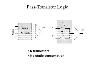
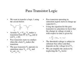
Pass-Transistor Logic Prof. V. G. Oklobdzija: High-Performance System Design
Pass-Transistor Logic (a) (b) • XOR function implemented with pass-transistor circuit • Karnaough map showing derivation of the XOR function Prof. V. G. Oklobdzija: High-Performance System Design
Pass-Transistor Logic General topology of pass-transistor function generator Karnaough map of 16 possible functions that can be realized Prof. V. G. Oklobdzija: High-Performance System Design
Pass-Transistor Logic Function generator implemented with pass-transistor logic Prof. V. G. Oklobdzija: High-Performance System Design
Pass-Transistor Logic Threshold voltage drop at the output of the pass-transistor gate Voltage drop does not exceed Vth when there are multiple transistors in the path Prof. V. G. Oklobdzija: High-Performance System Design
Pass-Transistor Logic • Elimination of the threshold voltage drop by: • pairing nMOS transistor with a pMOS • (b) using a swing-restoring inverter Prof. V. G. Oklobdzija: High-Performance System Design
Complementary Pass-Transistor Logic (CPL) Prof. V. G. Oklobdzija: High-Performance System Design
Basic logic functions in CPL Prof. V. G. Oklobdzija: High-Performance System Design
CPL Logic XOR gate Sum circuit CPL provides an efficient implementation of XOR function Prof. V. G. Oklobdzija: High-Performance System Design
CPL Inverter Prof. V. G. Oklobdzija: High-Performance System Design
Double Pass-Transistor Logic (DPL): AND/NAND XOR/XNOR Prof. V. G. Oklobdzija: High-Performance System Design
Double Pass-Transistor Logic (DPL): XOR One bit full-adder: Sum circuit Prof. V. G. Oklobdzija: High-Performance System Design
Double Pass-Transistor Logic (DPL): DPL Full Adder The critical path traverses two transistors only (not counting the buffer) Prof. V. G. Oklobdzija: High-Performance System Design
Formal Method for CPL Logic DerivationMarkovic et al. 2000 • (a) Cover the Karnaugh-map with largest possible cubes (overlapping allowed) • (b) Express the value of the function in each cube in terms of input signals • Assign one branch of transistor(s) to each of the cubes and connect all the branches to one common node, which is the output of NMOS pass-transistor network Prof. V. G. Oklobdzija: High-Performance System Design
Formal Method for P-T Logic Derivation Complementary function can be implemented from the same circuit structure by applying complementarity principle: Complementarity Principle:Using the same circuit topology, with pass signals inverted, complementary logic function is constructed in CPL. By applying duality principle, a dual function is synthesized: Duality Principle:Using the same circuit topology, with gate signals inverted, dual logic function is constructed. Following pairs of basic functions are dual: AND-OR (and vice-versa) NAND-NOR (and vice-versa) XOR and XNOR are self-dual (dual to itself) Prof. V. G. Oklobdzija: High-Performance System Design
Derivation of P-T Logic Copmplementarity: AND NAND; Duality: AND OR Prof. V. G. Oklobdzija: High-Performance System Design
Derivation of CPL Logic Complementarity: AND NAND Duality: AND OR NAND NOR Prof. V. G. Oklobdzija: High-Performance System Design
Two-Input Function with balanced input load Each input A, B, or A, B has FO=2 Prof. V. G. Oklobdzija: High-Performance System Design
Derivation of CPL Logic (a) XOR function Karnaugh map, (b) XOR/XNOR circuit Prof. V. G. Oklobdzija: High-Performance System Design
Synthesis of three-input CPL logic (a) AND function Karnaugh map, (b) AND/NAND circuit Prof. V. G. Oklobdzija: High-Performance System Design
Circuit realization of 3-input AND/NAND function Prof. V. G. Oklobdzija: High-Performance System Design
Double Pass-Transistor Logic (DPL): Synthesis Rules • Two NMOS branches can not be overlapped covering logic 1s. Similarly, two PMOS branches can not be overlapped covering logic 0s. • Pass signals are expressed in terms of input signals or supply. Every input vector has to be covered with exactly two branches. • At any time, excluding transitions, exactly two transistor branches are active (any of the pairs NMOS/PMOS, NMOS/NMOS and PMOS/PMOS are possible), i.e. they both provide output current. Prof. V. G. Oklobdzija: High-Performance System Design
Double Pass-Transistor Logic (DPL): Synthesis Rules • Complementarity Principle:Complementary logic function in DPL is generated after the following modifications: • Exchange PMOS and NMOS devices. Invert all pass and gate signals • Duality Principle:Dual logic function in DPL is generated when: • PMOS and NMOS devices are exchanged, and VDD and GND signalsare exchanged. Prof. V. G. Oklobdzija: High-Performance System Design
DPL Synthesis: (a) AND function Karnaugh map (b) AND/NAND circuit Prof. V. G. Oklobdzija: High-Performance System Design
DPL Synthesis: OR/NOR circuit Prof. V. G. Oklobdzija: High-Performance System Design
XOR/XNOR in DPL Circuit realization of 2-input XOR/XNOR function in DPL, with balanced input load Prof. V. G. Oklobdzija: High-Performance System Design
DPL Synthesis: Complementarity Principle:Exchange PMOS and NMOS devices. Invert all pass and gate signals AND NAND AND function Karnaugh map AND/NAND circuit Duality Principle:PMOS and NMOS devices are exchanged, and VDD and GND signalsare exchanged: AND OR NAND NOR Prof. V. G. Oklobdzija: High-Performance System Design
DVL Logic Advantage of CPL and DPL were recognized in DVL which attempts to generalize pass-transistor networks and minimize the number of transistors and input loads. Rules: Prof. V. G. Oklobdzija: High-Performance System Design
Two input AND/NAND in DVL Logic Circuit realization of 2-input AND/NAND function in DVL Prof. V. G. Oklobdzija: High-Performance System Design
Two input OR/NOR in DVL Logic Circuit realization of 2-input OR/NOR circuit in DVL XOR/XNOR realization is identical to that of DPL. Prof. V. G. Oklobdzija: High-Performance System Design
Three input AND function in DVL Logic Prof. V. G. Oklobdzija: High-Performance System Design
Three input OR/NOR in DVL Circuit realization of 3-input OR/NOR functions in DVL Prof. V. G. Oklobdzija: High-Performance System Design
Comparison TABLE I. Realizations of 3-input function F=B’C+ABC’ Prof. V. G. Oklobdzija: High-Performance System Design
Comparison Realizations of 3-input function F=B’C+ABC’ (a) Standard CMOS, (b) DVL, (c) DVL Prof. V. G. Oklobdzija: High-Performance System Design
Conclusion General rules for synthesizing logic gates in three representative pass-transistor techniques were shown. An algorithmic way for generation of various circuit topologies (complementary and dual circuits) is discussed. Generation of circuits with balanced input loads is suitable for library based designs is possible if complementarity and commutative principles are applied. This lays the foundation for development of computer aided design (CAD) tools capable of generating fast and power-efficient pass-transistor logic. Prof. V. G. Oklobdzija: High-Performance System Design