Download
1 / 27
270 likes | 437 Views
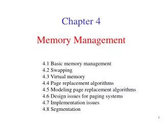
External Memory & I/O. External communications Designing an external 3 Byte Interface. You already have an external 1 Byte memory. * = INVERTED. Output Enable * (Read Data). Byte coming in (PORTA). Byte Stored (PORTE). CP (Write Data). Control lines (PORTD). Computer Bus.

E N D
External Memory & I/O External communications Designing an external 3 Byte Interface Mark Neil - Microprocessor Course
You already have an external 1 Byte memory * = INVERTED Output Enable* (Read Data) Byte coming in (PORTA) Byte Stored (PORTE) CP (Write Data) Control lines (PORTD) Mark Neil - Microprocessor Course
Computer Bus The processor within a computer communicates with the other computer modules via a device called: Bus. Many different Bus architectures exist in the market such as PCI; cPCI; VME…. All bus architectures include a control bus, a data bus and an address bus. Mark Neil - Microprocessor Course
The BUS of a computer: Bus Master (CPU/Controller) Bus Slave (e.g. Memory) Address Lines Data Lines Control Lines Mark Neil - Microprocessor Course
Typical Write Sequence The bus master places the address of the memory where the datum is to be written on the bus and validates it using the control lines. The master signals using the control lines that this is a write sequence. The master places the datum to be written onto the bus and validates it using the control lines. Each slave compares the address on the bus with its own address. If the write refers to it, it takes the data and signals (acknowledges) using the control lines that this has been done. Mark Neil - Microprocessor Course
Typical Read Sequence The master places the address of the memory from where the datum is to be read on the bus and validates it using the control lines. The master signals using the control lines that this is a read sequence. The master signals that it is ready to accept the datum using the control lines. The slave compares the address on the bus with its own address. If the read refers to it, it places the datum on the bus and validates it using the control lines (acknowledges the data). At the end the Master latches the datum. Mark Neil - Microprocessor Course
Parallel Transfer In a bus all bits of a byte or word are transferred simultaneously. If we have a byte wide bus and a transfer frequency of 1MHz then we have a bus speed of 1Mbytes/sec Hence, this is called Parallel Data Transfer (opposed to Serial Data Transfer that we will learn next) Mark Neil - Microprocessor Course
Interface to External SRAM Bus is implemented by using two of the ports! Mark Neil - Microprocessor Course
Electronics Exercise We will now make a 3 Byte interface that you can use for external read and write from/to the ATmega128 board. This is a challenging exercise and will take some time to construct and test Mark Neil - Microprocessor Course
High Level Design :3 Byte Memory We want to construct : Control and Address bus ATmega103 Board AS, READ WRITE, A0,A1 PORTD (Output Only) 1-Byte Memory 8-Bits of data_out 8-Bits of data_in PORTA (Output) 1-Byte Memory Data Bus Out 1-Byte Memory PORTE (Input) Data Bus In Mark Neil - Microprocessor Course
The data sheet for the 74F138 • You will need to select which memory chip to write to using a binary address • You will convert the 2 bits of “Address” into 3 lines which can be used to control the Enable lines for the three memory chips • To do this use an address decoder • The 74F138 converts a 3 bit address into 8 control output lines • When a given 3 bit number is written on the Address lines one of the 8 output lines is set high Mark Neil - Microprocessor Course
The 74F138 truth table Mark Neil - Microprocessor Course
Memory Design Data to write to the memory is placed on PORTAand this is wired to the memory Data Bus The data is read from the memories into PORTEfrom the output Data Bus The control lines for all this are sent on PORTD PORTA PORTE Mark Neil - Microprocessor Course
Control Bus We need to set four signals to control the memories A0:A1 – The Address Bits. These are used to define which memory chip will be addressed (00,01,10) AS* – The address strobe to select the memory R*/W to Read/Write the selected memory\ We will use bits on PORTD to control these signals – you chose which bits are attached to which control line Mark Neil - Microprocessor Course
Basic Circuit Control Signals AS,A1,A0 R/W On PORTD Output Data Bus (O0-O7) on PORTE Input Data (D0-D7) Bus – from PORTA Mark Neil - Microprocessor Course
Logic Gates • You will also use some basic logic gates in your circuit to build the control bus • 74HC04 Hex Not • 74HC08 Quad And • 74HC32 Quad OR Mark Neil - Microprocessor Course
Logic Table for Control Bus To read a memory, Address it on A0/A1 set AS* to 0 set R*W to 0 To Write a memory, Address it on A0/A1 Set AS* to 0 Change R*W from 0 to 1 Make sure you understand the Logic table and how it is implemented using the logic gates Exercise: Fill in the Table for Read2*/Write2 Mark Neil - Microprocessor Course
Sequence Diagram: Unneccessary - need another D-Flip-Flop to remove Mark Neil - Microprocessor Course
The Memory Test Program Start Enable memory 1 output Set data pattern on PORTA Copy PINE to PORTB LEDs Clock in memory 1 Enable memory 2 output Set data pattern on PORTA Copy PINE to PORTB LEDs Clock in memory 2 Set data pattern on PORTA Enable memory 3 output Clock in memory 3 Copy PINE to PORTB LEDs Mark Neil - Microprocessor Course
Task Plan: • Construct the 3 byte memory and connect it to your ATmage128 Board • Always connect to the ports through the special cable-resistor-pack units • Proceed in steps: • First the Control Bus, test it and verify that it works! • Next add the first memory byte and test it • Add the secondmemory and test it • Add the thirdmemory and test it • Write programs as you go along with the aid of a top-down-modular diagram • Use a main section • Use driver subroutines that read, write, and loop data through your memory bytes. Mark Neil - Microprocessor Course
Some Comments: • Make a detailed schematic of your device with all ICs (logic diagrams) and the IC pin assignments. • Make sure that you understand your design BEFORE you start building it. • Build the device in pieces which you can check using your software. Don’t build the entire design before testing. • Follow the steps – don’t leap ahead and build too much before checking that everything works at each step. • Use the oscilloscope and the DVM to check what is going on and debug your device. Mark Neil - Microprocessor Course
How to Draw Schematics: Mark Neil - Microprocessor Course
Step 1: The control bus Address lines Start by setting the Address Strobe* high Set the correct address on your bus. Now lower the AS* and check that the appropriate output bits are selected for the address of each memory Mark Neil - Microprocessor Course
The control bus Read/Write • Add the Read/Write control logic • First build Read0*/Write0 • Set AS*high and R*/Whigh. • Set the address on your bus • Lower R*W and AS* • This is a read memory setting • Check that Read0*/Write0 are what you expect • Bring *R/WHigh for 250 nsecand then back Low • This is a write memory • Use a scope to verify the timing • Complete the Read1*/Write1 and Read2*/Write2 circuits • Test that they are working as expected when you select each of the memory addresses. • you are ready to add a memory • Don’t this before your control bus works! Mark Neil - Microprocessor Course
Step 3: Adding the first memory • Connect the Data Bus (D0-D7) to the 8 bits on PORTA • Connect the OE* to the Read* and CP to the Write lines of your control bus • Using your program • Set AS*high and R*/W high . • Set the correct address and put some data on your bus. • Lower R*/W and AS* • Bring R*/W high for 250 nsecand then back to Low • Your data should now be stored in the selected register, and visible on the outputs • Before you connect the output together use scope/LED+Resistors to check if the data are on the outputs and correct • Connect the Output Bus to the pins on PORTE • Try reading the data with the AVR Mark Neil - Microprocessor Course
Step 4 Add the second Memory Chip Verify that it is working as expected Finally Add the third memory chip You should now be able to write data to the memory of your choice, and verify that it is properly stored Mark Neil - Microprocessor Course
Here is an example… When you build your board Think about Where inputs arrive Where the outputs go Where the memory buses will be Where the control bus will be What color wire you will use for what function Mark Neil - Microprocessor Course