Download
1 / 31
310 likes | 314 Views
This lecture reviews circuit concepts including passive devices, load lines, RC transients, Kirchhoff's current and voltage laws, nodal analysis, voltage dividers, series and parallel combinations, and Thévenin's theorem.

E N D
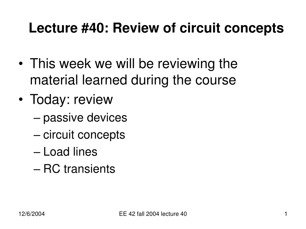
Lecture #40: Review of circuit concepts • This week we will be reviewing the material learned during the course • Today: review • passive devices • circuit concepts • Load lines • RC transients EE 42 fall 2004 lecture 40
branch (circuit element) BRANCHES AND NODES Circuit with several branches connected at a node: KIRCHOFF’s CURRENT LAW (Sum of currents entering node) (Sum of currents leaving node) = 0 q = charge stored at node is zero. If charge is stored, for example in a capacitor, then the capacitor is a branch and the charge is stored there NOT at the node. EE 42 fall 2004 lecture 40
GENERALIZATION OF KCL TO SURFACES Sum of currents entering and leaving any “black box” is zero Could be a big chunk of circuit in here, e.g., could be a “Black Box” In other words there can be lots of nodes and branches inside the box. EE 42 fall 2004 lecture 40
surface Another example 50 mA entering leaving m 5 A i = ? m 2 A i? KIRCHHOFF’S CURRENT LAW USING SURFACES Example i=7mA i must be 50 mA EE 42 fall 2004 lecture 40
a + v1 v2 + (since it’s the reference) c b d select as ref. “ground” e BRANCH AND NODE VOLTAGES The voltage across a circuit element is defined as the difference between the node voltages at its terminals Specifying node voltages: Use one node as the implicit reference (the “common” node … attach special symbol to label it) Now single subscripts can label voltages: e.g., vb means vb ve, va means va ve, etc. EE 42 fall 2004 lecture 40
Path Path + - “rise” or “step up” (negative drop) “drop” V V 2 1 + - KIRCHHOFF’S VOLTAGE LAW (KVL) The algebraic sum of the “voltage drops” around any “closed loop” is zero. Why? We must return to the same potential (conservation of energy). Voltage drop defined as the branch voltage if the + sign is encountered first; it is (-) the branch voltage if the sign is encountered first … important bookkeeping Closed loop: Path beginning and ending on the same node EE 42 fall 2004 lecture 40
Choose a Reference Node FORMAL CIRCUIT ANALYSIS USING KCL:NODAL ANALYSIS 2Define unknown node voltages (those not fixed by voltage sources) • Write KCL at each unknown node, expressing current in terms of the node voltages (using the constitutive relationships of branch elements) • Solve the set of equations (N equations for N unknown node voltages) EE 42 fall 2004 lecture 40
R1 V2 • Choose reference node i1 + V2 i2 + R2 • Define unknown node voltages VSS • Write KCL at unknown nodes • Solve: NODAL ANALYSIS USING KCL–Example: The Voltage Divider – This is of course the voltage divider formula and is by itself very useful. EE 42 fall 2004 lecture 40
I V1 ? R 1 R 2 VSS + + + • Thus, V3? R 3 R 4 and GENERALIZED VOLTAGE DIVIDER(solved without Nodal Analysis) Circuit with several resistors in series • We know etc.. etc.. EE 42 fall 2004 lecture 40
I I + R R 1 1 + R V R 2 Z 2 - - + + X V V SS SS - - i R R 3 3 3 R 5 R R 4 4 R R Correct if nothing else 2 V × V 2 ¹ × V V = 2 SS Z SS + + + connected to nodes R R R R 1 2 3 4 R + R + R + R 1 2 3 4 removes condition of because R 5 ¹ i I resistors in series – i.e. 3 What is V ? Z R Answer: 2 × V SS + + + R R R ( R R ) 1 2 5 3 4 WHEN IS VOLTAGE DIVIDER FORMULA CORRECT? V2 EE 42 fall 2004 lecture 40
VX • Select Reference Node I I 2 1 • Define unknown node voltages ISS R R 2 1 Note: Iss = I1 + I2, i.e., RESULT 2 RESULT 1 EQUIVALENT RESISTANCE: CURRENT DIVIDER: RESISTORS IN PARALLEL EE 42 fall 2004 lecture 40
R 1 I I R 3 R 2 V R 4 + R 6 R 5 parallel + RX ? IDENTIFYING SERIES AND PARALLEL COMBINATIONS Use series/parallel equivalents to simplify a circuit before starting KVL/KCL EE 42 fall 2004 lecture 40
R2 R1 and R2 are not in || R1 R3 V R5 R4 + IDENTIFYING SERIES AND PARALLEL COMBINATIONS(cont.) Some circuits must be analyzed (not amenable to simple inspection) R1 and R5 are not in series Special cases: R3 = 0 OR R3 = Req = R1 || R2 + R4 || R5 Example: R3 = 0 R1 || R2; R4 || R5 in series; OR IF R3 = (R1 + R5) || (R2 + R4) EE 42 fall 2004 lecture 40
+ TWO-TERMINAL LINEAR RESISTIVE NETWORKS(“One Port” Circuit) Model of two-terminal linear resistive elements with only two “accessible” terminals Replace a complicated circuit with a simple model a b EE 42 fall 2004 lecture 40
BASIS OF THÉVENIN THEOREM • All linear one-ports have linear I-V graph • A voltage source in series with a resistor can produce any linear I-V graph by suitably adjusting V and I THUS We define the voltage-source/resistor combination that replicates the I-V graph of a linear circuit to be the Thévenin equivalent of the circuit. The voltage source VT is called the Thévenin equivalent voltage and the resistance RT is called the Thévenin equivalent resistance. EE 42 fall 2004 lecture 40
Apply v, measure i, or vice versa i(mA) Associated (i defined in) 1 i .5 + + 5V v v(V) 5 -.5 -1 I-V CHARACTERISTICS OF LINEAR TWO-TERMINAL NETWORKS 5K What is the easy way to find the I-V graph? Associated First find open-circuit V v=5V if i = 0 Now find Short-circuit I i = -1mA if v = 0 EE 42 fall 2004 lecture 40
Apply v, measure i, or vice versa i If V = 2.5V + + 5V v If R = 2.5K I-V CHARACTERISTICS OF LINEAR TWO-TERMINAL NETWORKS 5K Consider how the graph changes with differences in V and R. i(mA) 1 .5 First consider change in V, eg V= 2.5V, not 5V v(V) 5 -.5 Now consider change in R (with V back at 5V) -1 Clearly by varying V and R we can produce an arbitrary linear graph … in other words this circuit can produce any linear graph EE 42 fall 2004 lecture 40
i i RT + Any linear circuit + V V This circuit is equivalent to any circuit, that is by suitably choosing VT and RT it will have the same I-V graph VT + Thévenin Equivalent Circuit So how do we choose VT and RT ? EE 42 fall 2004 lecture 40
R I N N NORTON EQUIVALENT CIRCUIT Corollary to Thévenin: (associated) RN is found the same way as for Thévenin equivalent i + V - EE 42 fall 2004 lecture 40
A 2 K 2 K + 2 V B A 1K A + - 1V 1 mA 1 K B B EXAMPLE 1, Continued In what sense is this circuit equivalent to these? • They have identical I-V characteristics and therefore have • The same open circuit voltage • The same short circuit current • For any voltage, they will produce the same current • And visa versa EE 42 fall 2004 lecture 40
(ma) I 2.5V I Solution: I = 0.5mA, V = 2.5V 4 1K + - + - Combined 1K + 4K 2.5V V 4K 2 V (Volt) 5 Load line method We can find the currents and voltages in a simple circuit graphically. For example if we apply a voltage of 2.5V to the two resistors of our earlier example: We draw the I-V of the voltage and the I-V graph of the two resistors on the same axes. Can you guess where the solution is? At the point where the voltages of the two graphs AND the currents are equal. (Because, after all, the currents are equal, as are the voltages.) EE 42 fall 2004 lecture 40
I (ma) I + - Solution: I = 0.7mA, V = 1.4V 2V 4 V 2K 2 V (Volt) 5 Another Example of the Load-Line Method Lets hook our 2K resistor + 2V source circuit up to an LED (light-emitting diode), which is a very nonlinear element with the IV graph shown below. Again we draw the I-V graph of the 2V/2K circuit on the same axes as the graph of the LED. Note that we have to get the sign of the voltage and current correct!! At the point where the two graphs intersect, the voltages and the currents are equal, in other words we have the solution. LED + - LED EE 42 fall 2004 lecture 40
input voltage time voltage output time Simplification for time behavior of RC Circuits Before any input change occurs we have a dc circuit problem (that is we can use dc circuit analysis to relate the output to the input). Long after the input change occurs things “settle down” …. Nothing is changing …. So again we have a dc circuit problem. We call the time period during which the output changes the transient We can predict a lot about the transient behavior from the pre- and post-transient dc solutions EE 42 fall 2004 lecture 40
V1 Vin R Input node Output node Vout + Vout C Vin 0 time - 0 ground RC RESPONSE Case 1 – Rising voltage. Capacitor uncharged: Apply + voltage step • Vin “jumps” at t=0, but Vout cannot “jump” like Vin. Why not? • Because an instantaneous change in a capacitor voltage would require instantaneous increase in energy stored (1/2CV²), that is, infinite power. (Mathematically, V must be differentiable: I=CdV/dt) V does not “jump” at t=0 , i.e. V(t=0+) = V(t=0-) The dc solution before the transient tells us the capacitor voltage at the beginning of the transient. EE 42 fall 2004 lecture 40
V1 Vin R Input node Output node Vout + Vout C Vin 0 time - 0 ground RC RESPONSE Case 1 Continued – Capacitor uncharged: Apply voltage step • Vout approaches its final value asymptotically (It never actually gets exactly to V1, but it gets arbitrarily close). Why? After the transient is over (nothing changing anymore) it means d(V)/dt = 0 ; that is all currents must be zero. From Ohm’s law, the voltage across R must be zero, i.e. Vin = Vout. • That is, Vout V1 as t . (Asymptotic behavior) Again the dc solution (after the transient) tells us (the asymptotic limit of) the capacitor voltage during the transient. EE 42 fall 2004 lecture 40
5 Vin R Input node Output node Vout + Vout C Vin 0 time - 0 ground RC RESPONSE Example – Capacitor uncharged: Apply voltage step of 5 V • Clearly Vout starts out at 0V ( at t = 0+) and approaches 5V. • We know this because of the pre-transient dc solution (V=0) and post-transient dc solution (V=5V). So we know a lot about Vout during the transient - namely its initial value, its final value , and we know the general shape . EE 42 fall 2004 lecture 40
at t = 0, Vout = 0 , and at t , Vout V1 also at t = t, Vout = 0.63 V1 at t = 0, Vout = V1 , and at t , Vout 0, also at t = t, Vout = 0.37 V1 8 8 Vout Vout V1 V1 .63V1 .37V1 0 0 time 0 time t 0 t Review of simple exponentials. Rising Exponential from Zero Falling Exponential to Zero Vout = V1(1-e-t/t) Vout = V1e-t/t EE 42 fall 2004 lecture 40
Vout Vout V1 + V2 V1 + V2 .63V1+ V2 .37V1 + V2 V2 V2 0 time 0 t 0 time 0 t Further Review of simple exponentials. Rising Exponential from Zero Falling Exponential to Zero Vout = V1(1-e-t/t) Vout = V1e-t/t We can add a constant (positive or negative) Vout = V1(1-e-t/t) + V2 Vout = V1e-t/t + V2 EE 42 fall 2004 lecture 40
Vout = A + Be-t/t Vout Vout A A+B Here B > 0 Here B < 0 A+B A 0 0 time 0 time 0 Further Review of simple exponentials. Rising Exponential Falling Exponential Vout = V1e-t/t + V2 Vout = V1(1-e-t/t) + V2 Both equations can be written in one simple form: Initial value (t=0) : Vout = A + B. Final value (t>>t): Vout = A Thus: if B < 0, rising exponential; if B > 0, falling exponential EE 42 fall 2004 lecture 40
Capacitance to Ground D Actual exponential voltage versus time. LOGIC GATE DELAY D Time delay D occurs between input and output: “computation” is not instantaneous Value of input at t = 0+ determines value of output at later time t = D F A B Logic State Input (A and B tied together) 1 0 t 0 Output (Ideal delayed step-function) 1 F t 0 0 EE 42 fall 2004 lecture 40
Oscilloscope Probe Note B changes one gate delay after A switches Note that C changes two gate delays after A switches. Note that D changes three gate delays after A switches. t 2t 3t t SIGNAL DELAY: TIMING DIAGRAMS Show transitions of variables vs time B C A D Logic state 1 A t 0 0 B t t C t t 2t D EE 42 fall 2004 lecture 40