Download
1 / 35
350 likes | 435 Views
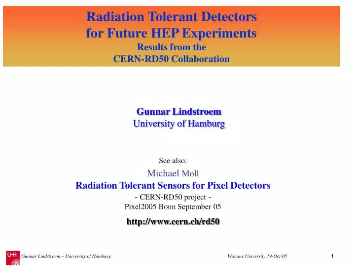
Radiation Tolerant Detectors for Future HEP Experiments Results from the CERN-RD50 Collaboration. Gunnar Lindstroem University of Hamburg. See also: Michael Moll Radiation Tolerant Sensors for Pixel Detectors - CERN-RD50 project - Pixel2005 Bonn September 05 http://www.cern.ch/rd50.

E N D
Radiation Tolerant Detectors for Future HEP Experiments Results from the CERN-RD50 Collaboration Gunnar LindstroemUniversity of Hamburg See also: Michael Moll Radiation Tolerant Sensors for Pixel Detectors- CERN-RD50 project - Pixel2005 Bonn September 05http://www.cern.ch/rd50 Warsaw University 19-Oct-05
Outline • Silicon Detectors for Particle Tracking • Motivation for R&D, the Challenge for Radiation Tolerance • The RD50 Collaboration • Radiation Damage, Deterioration of Detector Properties • Approaches for Solutions, Material and Device Engineering • Summary and Outlook Warsaw University 19-Oct-05
Reliable detection of mips S/N ≈ 10 reachable with Experimental requestDetector property Proton-proton collider Energy: 2 x 7 TeV Luminosity: 1034 Bunch crossing: every 25 nsec Rate: 40 MHz pp-collision event rate: 109/sec (23 interactions per bunch crossing) Annual operational period: 107 sec Expected total op. period: 10 years LHC properties period of 10 years low dissipation power atmoderate cooling Silicon pixel and microstrip detectors meet all requirements for LHC How about future developments? LHC-Challenge for Tracking Detectors employing minimum minimum detectorthickness material budget High event rate excellent time- (~10 ns) & high track accuracy & position resolution (~10 µm) Silicon Detectors: Favorite Choice for Particle Tracking Proton-proton collider, 2 x 7 TeV Luminosity: 1034 Bunch crossing: every 25 nsec, Rate: 40 MHz event rate: 109/sec (23 interactions per bunch crossing) Annual operational period: 107 sec Expected total op. period: 10 years LHC properties Experimental requests Detector properties Reliable detection of mips S/N ≈ 10 High event rate time + positionresolution: high track accuracy~10 ns and ~10 µm Complex detector design low voltage operation in normal ambients Intense radiation field Radiation tolerance up to during 10 years 1015 hadrons/cm² Feasibility, e.g.large scale availability 200 m² for CMSknown technology, low cost ! Silicon Detectors meet all Requirements ! Warsaw University 19-Oct-05 Intense radiation field Radiation tolerance up to throughout operational 1015 1MeV eq. n/cm²
LHC ATLAS Detector – a Future HEP Experiment Overall length: 46m, diameter: 22m, total weight: 7000t, magnetic field: 2T ATLAS collaboration: 1500 members principle of a silicon detector: solid state ionization chamber micro-strip detectorfor particle tracking Warsaw University 19-Oct-05
Growing demand for Si-detectors in tracking applications Covered area in m² Warsaw University 19-Oct-05
5 years 10 years 2500 fb-1 500 fb-1 Main motivations for R&D on Radiation Tolerant Detectors: Super - LHC RD50 • LHC upgradeLHC (2007), L = 1034cm-2s-1f(r=4cm) ~3·1015cm-2 • Super-LHC (2015 ?), L = 1035cm-2s-1f(r=4cm) ~1.6·1016cm-2 • LHC (Replacement of components)e.g. - LHCb Velo detectors (~2010) - ATLAS Pixel B-layer (~2012) • Linear collider experiments (generic R&D)Deep understanding of radiation damage will be fruitful for linear collider experiments where high doses of e, g will play a significant role. 5 CERN-RD48 CERN-RD50 Adopted from M. Moll,CERN, Bonn, Sep-05 Warsaw University 19-Oct-05
The CERN RD50 Collaboration http://www.cern.ch/rd50 RD50 RD50:Development of Radiation Hard Semiconductor Devices for High Luminosity Colliders • Collaboration formed in November 2001 • Experiment approved as RD50 by CERN in June 2002 • Main objective: Development of ultra-radiation hard semiconductor detectors for the luminosity upgrade of the LHC to 1035 cm-2s-1 (“Super-LHC”). Challenges: - Radiation hardness up to 1016 cm-2 required - Fast signal collection (Going from 25 ns to 10 ns bunch crossing ?) - Low mass (reducing multiple scattering close to interaction point) - Cost effectiveness (big surfaces have to be covered with detectors!) Presently 251 members from 51 institutes Belarus (Minsk), Belgium (Louvain), Canada (Montreal), Czech Republic (Prague (3x)), Finland (Helsinki, Lappeenranta), Germany (Berlin, Dortmund, Erfurt, Freiburg, Hamburg, Karlsruhe), Israel (Tel Aviv), Italy (Bari, Bologna, Florence, Padova, Perugia, Pisa, Trento, Turin), Lithuania (Vilnius), Norway (Oslo (2x)), Poland (Warsaw(2x)), Romania (Bucharest (2x)),Russia (Moscow), St.Petersburg), Slovenia (Ljubljana), Spain (Barcelona, Valencia), Switzerland (CERN, PSI), Ukraine (Kiev), United Kingdom(Exeter, Glasgow, Lancaster, Liverpool, Sheffield, University of Surrey), USA (Fermilab, Purdue University, Rochester University, SCIPP Santa Cruz, Syracuse University, BNL, University of New Mexico) Adopted from M. Moll,CERN, Bonn, Sep-05 Warsaw University 19-Oct-05
Defect / Material CharacterizationBengt Svensson(Oslo University) Defect EngineeringEckhart Fretwurst(Hamburg University) New MaterialsJuozas V.Vaitkus(Vilnius University) Macroscopic EffectsJaakko Härkönen(Helsinki HIP) New StructuresMahfuzur Rahman (Glasgow University) Full DetectorSystemsGianluigiCasse (Liverpool University) • Characterization: (pre/post irradiation) SIMS, IR, PL, Hall, TSC, DLTS, EPR,… - V2O, O-dimers,… - high res. CZ, … - clusters, .. • Theory: Defect formation, defect annealing, energy states,….. • DOFZ/Oxygenation • High resistivity CZ • Epitaxial Silicon • Dimerization • Other impurities H, N, Ge, … • Thermal donors • Pre-irradiation treatments • SiC • CdTe • other materials • Test structure characterizationIV, CV, CCE • NIEL • Device modeling • Operational conditions • 3D detectors • Thin detectors • Cost effective solutions • LHC-like tests • Links to HEP • Links to R&D of electronics • Comparison: pad-mini-full detectors Scientific Organization of RD50 SpokespersonMara BruzziINFN and University of Florence Deputy-SpokespersonMichael MollCERN CERN contact: Michael Moll Warsaw University 19-Oct-05
Radiation Damage in Silicon Sensors • Two general types of radiation damage in detector materials:Bulk (Crystal) damagedue to Non Ionizing Energy Loss (NIEL) - displacement damage, built up of crystal defects – • I. Change of effective doping concentration(higher depletion voltage, under- depletion)II. Increase of leakage current (increase of shot noise, thermal runaway) • III. Increase of charge carrier trapping(loss of charge) • Surface damagedue to Ionizing Energy Loss (IEL)- accumulation of positive in the oxide (SiO2) and the Si/SiO2 interface – affects: interstrip capacitance (noise factor), breakdown behavior, … • Impact on detector performance and Charge Collection (depending on detector type and geometry and readout electronics!)Signal/noise ratio is the quantity to watch • Sensors can fail from radiation damage ! Adopted from M. Moll,CERN, Bonn, Sep-05 Warsaw University 19-Oct-05
Non Ionizing Energy Loss NIEL: displacement damage Point defects + clusters Dominated by clusters Damage effects generally ~ NIEL, however differences betweenproton&neutron damage Warsaw University 19-Oct-05
…. with time (annealing): Short term: “Beneficial annealing”Long term: “Reverse annealing” - time constant depends on temperature:~ 500 years (-10°C)~ 500 days ( 20°C)~ 21 hours ( 60°C) - Consequence: Detectors must be cooled even when the experiment is not running! Radiation Damage I. – Effective doping concentration • Change of Depletion Voltage Vdep (Neff)…. with particle fluence: „Hamburg model“ “Type inversion”: Neff changes from positive to negative (Space Charge Sign Inversion) afterinversion before inversion p+ n+ n+ p+ Warsaw University 19-Oct-05
…. with time (annealing): 80 min 60C Radiation Damage II. – Leakage current • Change of Leakage Current (after hadron irradiation)…. with particle fluence: • Leakage current decreasing in time (depending on temperature) • Strong temperature dependence: • Damage parameter (slope in figure)Leakage current per unit volume and particle fluence • is constant over several orders of fluenceand independent of impurity concentration in Si can be used forfluence measurement Consequence:Cool detectors during operation! Example: I(-10°C) ~1/16 I(20°C) Warsaw University 19-Oct-05
….. and change with time (annealing): Radiation Damage III. – Charge carrier trapping • Deterioration of Charge Collection Efficiency (CCE) by trapping Trapping is characterized by an effective trapping time eff for electrons and holes: where: Increase of inverse trapping time (1/) with fluence Adopted from M. Moll,CERN, Bonn, Sep-05 Warsaw University 19-Oct-05
Impact on Detector: Decrease of CCE • Two basic mechanisms reduce collectable charge: • - trapping of electrons and holes (depending on drift and shaping time !) - under-depletion (depending on detector design and geometry !) • Example: ATLAS microstrip detectors + fast electronics (25ns) p-in-n : oxygenated versus standard FZ- beta source- 20% charge loss after 5x10¹⁴ p/cm2 (23 GeV) n-in-n versus p-in-n- same material, ~ same fluence- over-depletion needed Adopted from M. Moll,CERN, Bonn, Sep-05 Warsaw University 19-Oct-05
Approaches for Radiation Hardening • Defect Engineering of Silicon • Understanding radiation damage • Macroscopic effects and Microscopic defects • Simulation of defect properties & kinetics • Irradiation with different particles & energies • Oxygen rich Silicon • DOFZ, Cz, MCZ, EPI • Oxygen dimer & hydrogen enriched Si • Pre-irradiated Si • Influence of processing technology • New Materials • Silicon Carbide (SiC), Gallium Nitride (GaN) • Diamond: CERN RD42 Collaboration • Amorphous silicon • Device Engineering (New Detector Designs) • p-type silicon detectors (n-in-p) • thin detectors • 3D and Semi 3D detectors • Stripixels • Cost effective detectors • Simulation of highly irradiated detectors • Monolithic devices Scientific strategies: I. Material engineering II. Device engineering III. Change of detectoroperational conditions CERN-RD39“Cryogenic Tracking Detectors”„Lazarus Effect“ Adopted from M. Moll,CERN, Bonn, Sep-05 Warsaw University 19-Oct-05
Different Sensor mMaterials Example: is SiC an option? Wide bandgap (3.3eV) lower leakage current than silicon Signal:Diamond 36 e/mmSiC 51 e/mmSi 89 e/mm more charge than diamond Higher displacement threshold than silicon radiation harder than silicon (?) Result for SiC: very low CCE even for very thin devices R&D on diamond detectors:RD42 – Collaborationhttp://cern.ch/rd42/ Recent review: P.J.Sellin and J.Vaitkus on behalf of RD50 “New materials for radiation hard semiconductor detectors”, submitted to NIMA Adopted from M. Moll,CERN, Bonn, Sep-05 Warsaw University 19-Oct-05
Monocrystalline Material: Float Zone Silicon (FZ) • Float Zone process • Mono-crystalline Ingot Using a single Si crystal seed, meltthe vertically oriented rod onto the seed using RF power and “pull” themonocrystalline ingot • Wafer productionSlicing, lapping, etching, polishing • Oxygen enrichment (DOFZ)Oxidation of wafer at high temperatures Adopted from M. Moll,CERN, Bonn, Sep-05 Warsaw University 19-Oct-05
Czochralski Silicon (Cz) & Epitaxial Silicon (EPI) • Czochralski silicon • Pull Si-crystal from a Si-melt contained in a silica crucible while rotating. • Silica crucible is dissolving oxygen into the melt high concentration of O in CZ • Material used by IC industry (cheap) • Recent developments (~2 years) made CZ available in sufficiently high purity (resistivity) to allow for use as particle detector. • Epitaxial silicon • Chemical-Vapor Deposition (CVD) of Silicon • CZ silicon substrate used in-diffusion of oxygen • growth rate about 1m/min • excellent homogeneity of resistivity • up to 150 m thick layers produced (thicker is possible) • price depending on thickness of epi-layer but not extending ~ 3 x price of FZ wafer Adopted from M. Moll,CERN, Bonn, Sep-05 Warsaw University 19-Oct-05
Oxygen in FZ, Cz and EPI • Cz and DOFZ silicon • Epitaxial silicon • CZ: high Oi (oxygen) and O2i (oxygen dimer) concentration (homogeneous) • CZ: formation of Thermal Donors possible ! EPIlayer CZ substrate [G.Lindström et al.,10th European Symposium on Semiconductor Detectors, 12-16 June 2005] • DOFZ: inhomogeneous oxygen distribution • DOFZ: oxygen content increasing with time at high temperature • EPI: Oi and O2i (?) diffusion from substrate into epi-layer during production • EPI: in-homogeneous oxygen distribution Warsaw University 19-Oct-05
Change of Neff: FZ, DOFZ, Cz and MCz Silicon 24 GeV/c proton irradiation • Standard FZ silicon • type inversion at ~ 21013 p/cm2 • strong Neff increase at high fluence • Oxygenated FZ (DOFZ) • type inversion at ~ 21013 p/cm2 • reduced Neff increase at high fluence • CZ siliconand MCZ silicon • no type inversion in the overall fluence range (verified by TCT measurements)(verified for CZ silicon by TCT measurements, preliminary result for MCZ silicon) donor generation overcompensates acceptor generation in high fluence range • Common to all materials (after hadron irradiation): • reverse current increase • increase of trapping (electrons and holes) within ~ 20% Adopted from M. Moll,CERN, Bonn, Sep-05 Warsaw University 19-Oct-05
105V (25mm) 230V (50mm) 320V (75mm) Change of Neff: EPI Silicon G.Lindström et al.,10th European Symposium on Semiconductor Detectors, 12-16 June 2005 • Epitaxial silicon grown by ITME • Layer thickness: 25, 50, 75 m; resistivity: ~ 50 cm • Oxygen: [O] 91016cm-3; Oxygen dimers (detected via IO2-defect formation) • No type inversion in the full range up to ~ 1016 p/cm2 and ~ 1016 n/cm2 (type inversion only observed during long term annealing)Proposed explanation: introduction of shallow donors bigger than generation of deep acceptors Warsaw University 19-Oct-05
Epitaxial Silicon - Annealing • 50 mm thick silicon detectors:- Epitaxial silicon (50 Wcm on CZ substrate, ITME & CiS) - Thin FZ silicon (4KWcm, MPI Munich, wafer bonding technique) • Thin FZ silicon: Type inverted, increase of depletion voltage with time • Epitaxial silicon: No type inversion, decrease of depletion voltage with time No need for low temperature during maintenance of SLHC detectors! Adopted from M. Moll,CERN, Bonn, Sep-05 Warsaw University 19-Oct-05
Detector withcooling when notoperated Detector withoutcooling when notoperated Damage Projection – SLHC- 50 mm EPI silicon: a solution for pixels ?- G.Lindström et al.,10th European Symposium on Semiconductor Detectors, 12-16 June 2005 (Damage projection: M.Moll) • Radiation level (4cm):eq(year) = 3.5 1015 cm-2 • SLHC-scenario:1 year = 100 days beam (-7C) 30 days maintenance (20C) 235 days no beam (-7C or 20C) Warsaw University 19-Oct-05
Signal from irradiated EPI • Epitaxial silicon: CCE measured with beta particles (90Sr) • 25ns shaping time • proton and neutron irradiations of 50 mm and 75 mm epi layers CCE (75 mm) F=2x10¹⁵ n/cm-2,4500 electrons CCE (50 mm) Feq=8x10¹⁵ n/cm-2,2300 electrons CCE (50 mm): F=1x1016cm-2 (24GeV/c protons) 2400 electrons [G.Kramberger et al.,RESMDD - October 2004] Adopted from M. Moll,CERN, Bonn, Sep-05 Warsaw University 19-Oct-05
V SiS I particle I V I V Microscopic defects • Damage to the silicon crystal: Displacement of lattice atoms EK>25 eV Vacancy + Interstitial “point defects”, mobile in silicon,can react with impurities (O,C,..) EK > 5 keV point defects and defect clusters Distribution of vacancies created by a 50 keV Si-ion in silicon (typical recoil energy for 1 MeV neutrons):Schematic[Van Lint 1980] Simulation[M.Huhtinen 2001] • Defects can be electrically active (levels in the band gap)- capture and release electrons and holes from conduction and valence band can be charged - can be generation/recombination centers - can be trapping centers Adopted from M. Moll,CERN, Bonn, Sep-05 Warsaw University 19-Oct-05
Characterization of microscopic defects- gamma and proton irradiated silicon detectors - • 2003:Major breakthrough on g-irradiated samplesFor the first timemacroscopic changes of the depletion voltage and leakage currentcan be explained by electrical properties of measured defects ! • 2004:Big step in understanding the improved radiation tolerance of oxygen enriched and epitaxial silicon after proton irradiation [APL, 82, 2169, March 2003] [I.Pintilie, RESMDD, Oct.2004] Levels responsible for depletion voltage changes after proton irradiation: Almost independent of oxygen content: • Donor removal • “Cluster damage” negative chargeInfluenced by initial oxygen content: • I–defect: deep acceptor level at EC-0.54eV (good candidate for the V2O defect)negative chargeInfluenced by initial oxygen dimer content (?): • BD-defect: bistable shallow thermal donor (formed via oxygen dimers O2i) positive charge See further: I. Pintilie et al, NIM A 556 (2005) 56 + NIM A, in press Warsaw University 19-Oct-05
Device Engineering: p-in-n versus n-in-n n-type silicon after type inversion: p+on-n n+on-n • p-on-n silicon, under-depleted: • Charge spread – degraded resolution • Charge loss – reduced CCE • n-on-n silicon, under-depleted: • Limited loss in CCE • Less degradation with under-depletion • Collect electrons (fast) Adopted from M. Moll,CERN, Bonn, Sep-05 Warsaw University 19-Oct-05
n-in-p microstrip detectors n-in-p: - no type inversion, high electric field stays on segmented side - collection of electrons • Miniature n-in-p microstrip detectors (280mm) • Detectors read-out with LHC speed (40MHz) chip (SCT128A) • Material: standard p-type and oxygenated (DOFZ) p-type • Irradiation: G. Casse et al., NIMA 535 (2004) 362 At the highest fluence Q~6500e at Vbias=900V Feq = 4.6 1015 cm-2 CCE ~ 60% after 3 1015 p cm-2 at 900V( standard p-type) CCE ~ 30% after 7.5 1015 p cm-2 900V (oxygenated p-type) Adopted from M. Moll,CERN, Bonn, Sep-05 Warsaw University 19-Oct-05
Does thickness pay? • Low fluence Feq≤ 1014 cm-2:negligible trapping of charge carriers, signal for mip (minimum ionizing particle) proportinal to detector thickness:S ~ d • Trapping materialindependent, strong increase with fluence (see above) • Large fluence Feq≥ 5·1015 cm-2:signal height dominated by charge trapping, collection distance deff ≤ 100 mmsignal for mip: S ~ deff T. Lari, Milano 10 years at LHC Signal vs. Φeqfor 600V Signal vs. bias for Φeq = 1016 cm-2 Equiv. Fluence in 1015 cm-2 5 y S-LHC ! After Φeq = 1016 cm-2 S(mip) = about 2000-2500 e regardless of material and thickness ! Warsaw University 19-Oct-05
Summary • At fluences up to 1015cm-2(Outer layers of a SLHC detector)the change of depletionvoltage and the large area to be covered by detectors is the major problem. • CZ silicon detectors could be a cost-effective radiation hard solution (no type inversion, use p-in-n technology) • p-type siliconmicrostrip detectors show very encouraging results: CCE 6500 e; Feq=41015 cm-2, 300mm, collection of electrons, no reverse annealing observed in CCE measurement! • At the fluence of 1016cm-2(Innermost layer of a SLHC detector) the active thickness of any silicon material is significantly reduced due to trapping. The promising new options are:⁃Thin/EPIdetectors : drawback: radiation hard electronics for low signals needede.g. 2300e at Feq 8x1015cm-2, 50mm EPI, …. thicker layers will be tested in 2005/2006⁃ 3D detectors : drawback: technology has to be optimized ….. steady progress within RD50 • New Materials like SiC and GaN (not shown) have been characterized . ⁃ CCE tests show that these materials are not radiation harder than silicon Further information: http://cern.ch/rd50/ Adopted from M. Moll,CERN, Bonn, Sep-05 Warsaw University 19-Oct-05