Download
1 / 1
10 likes | 129 Views
Lyman-alpha. Target Features. Mold. MRI8030. Cr. SiO 2. Si. Oxide absorbs photons below 155nm. 2 nd imprint. References. Leskelä et al. (2007), Mater. Sci. Eng. C , 27, 1504–1508 Oehrlein and Kurogi (1998), Mat. Sci. Eng. R , 24 (4), 153–183

E N D
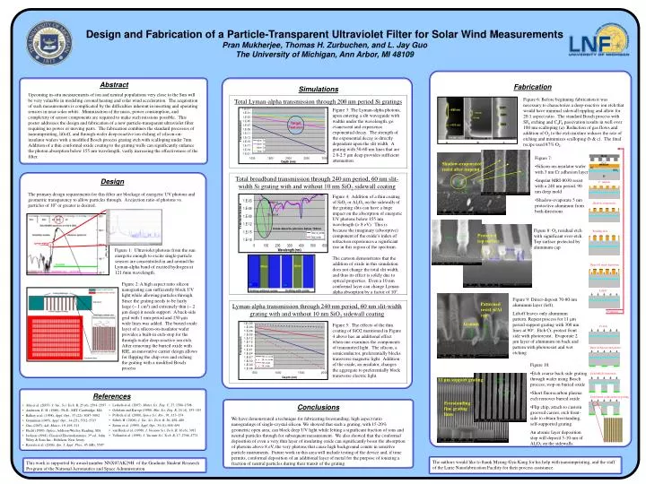
Lyman-alpha Target Features Mold MRI8030 Cr SiO2 Si Oxide absorbs photons below 155nm 2nd imprint References • Leskelä et al. (2007), Mater. Sci. Eng. C, 27, 1504–1508 • Oehrlein and Kurogi (1998), Mat. Sci. Eng. R, 24 (4), 153–183 • Pollock et al. (2000), Space Sci. Rev., 91, 113–154 • Schift, H. (2008), J. Vac. Sci. Tech. B, 26, 458–480 • Scime et al. (1995), Appl. Opt., 34 (4), 648–654 • van Beek et al. (1998), J. Vacuum Sci. Tech. B, 16 (6), 3911 • Volland et al. (1999), J. Vacuum Sci. Tech. B, 17, 2768–2771 Conclusions • Ahn et al. (2007), J. Vac. Sci. Tech. B, 25 (6), 2593–2597 • Anderson, E. H. (1988), Ph.D., MIT, Cambridge, MA • Balkey et al. (1998), Appl. Opt., 37 (22), 5087–5092 • Gruntman (1995), Appl. Opt., 34 (25), 5732–5737 • Guo (2007), Adv. Mater., 19, 495–513 • Hecht (1990), Optics, Addison-Wesley, Reading, MA • Jackson (1998), Classical Electrodynamics, 3rd ed., John Wiley & Sons Inc., Hoboken, New Jersey • Kawata et al. (2006), Jpn. J. Appl. Phys., 45 (6B), 5597 We have demonstrated a technique for fabricating freestanding, high aspect ratio nanogratings of single-crystal silicon. We showed that such a grating, with 15-20% geometric open area, can block deep UV light while letting a significant fraction of ions and neutral particles through for subsequent measurement. We also showed that the conformal deposition of even a very thin layer of insulating oxide can significantly boost the absorption of photons above 8 eV, the very photons that cause high background counts in sensitive particle instruments. Future work in this area will include testing of the device and, if time permits, conformal deposition of an additional layer of metal for the purpose of ionizing a fraction of neutral particles during their transit of the grating. This work is supported by award number NNX07AK29H of the Graduate Student Research Program of the National Aeronautics and Space Administration. The authors would like to thank Myung-Gyu Kang for his help with nanoimprinting, and the staff of the Lurie Nanofabrication Facility for their process assistance. Design and Fabrication of a Particle-Transparent Ultraviolet Filter for Solar Wind Measurements Pran Mukherjee, Thomas H. Zurbuchen, and L. Jay Guo The University of Michigan, Ann Arbor, MI 48109 Abstract Fabrication Simulations Upcoming in-situ measurements of ion and neutral populations very close to the Sun will be very valuable in modeling coronal heating and solar wind acceleration. The acquisition of such measurements is complicated by the difficulties inherent in inserting and operating sensors in near-solar orbits. Minimization of the mass, power consumption, and complexity of sensor components are required to make such missions possible. This poster addresses the design and fabrication of a new particle-transparent ultraviolet filter requiring no power or moving parts. The fabrication combines the standard processes of nanoimprinting, liftoff, and through-wafer deep-reactive ion etching of silicon-on-insulator wafers with a modified Bosch process grating etch with scalloping under 7nm. Addition of a thin conformal oxide coating to the grating walls can significantly enhance the photon absorption below 155 nm wavelength, vastly increasing the effectiveness of the filter. Figure 6: Before beginning fabrication it was necessary to characterize a deep-reactive ion etch that would have minimal sidewall rippling and allow for 20:1 aspect ratio. The standard Bosch process with SF6 etching and C4F8 passivation results in well over 100 nm scalloping (a). Reduction of gas flows and addition of O2 to the etch mixture reduces the rate of etching and minimizes scalloping (b & c). The final recipe used 87% O2. Total Lyman-alpha transmission through 200 nm period Si gratings Figure 3: The Lyman-alpha photons, upon entering a slit waveguide with widths under the wavelength, go evanescent and experience exponential decay. The strength of the exponential decay is directly dependent upon the slit width. A grating with 50-60 nm lines that are 2.0-2.5 μm deep provides sufficient attenuation. • Figure 7: • Silicon-on-insulator wafer with 3 nm Cr adhesion layer • Imprint MRI-8030 resist with a 240 nm period, 90 nm deep mold • Shadow-evaporate 5 nm protective aluminum from both directions. Shadow-evaporated resist after imprint Total broadband transmission through 240 nm period, 60 nm slit-width Si grating with and without 10 nm SiO2 sidewall coating Design 1st imprint The primary design requirements for this filter are blockage of energetic UV photons and geometric transparency to allow particles through. A rejection ratio of photons vs. particles of 105 or greater is desired. Figure 4: Addition of a thin coating of SiO2 or Al2O3 on the sidewalls of the grating slits can have a huge impact on the absorption of energetic UV photons below 155 nm wavelength (> 8 eV). This is because the imaginary (absorptive) component of the oxide’s index of refraction experiences a significant rise in this region of the spectrum. The cartoon demonstrates that the addition of oxide in this simulation does not change the total slit width, and thus its effect is solely due to optical properties. Even a 10 nm conformal layer can change Lyman-alpha absorption by a factor of 105. Shadow evaporation Figure 8: O2 residual etch with significant over-etch. Top surface protected by aluminum cap Residual etch Protected top surface Figure 1: Ultraviolet photons from the sun energetic enough to excite single-particle sensors are concentrated in and around the Lyman-alpha band of excited hydrogen at 121.6nm wavelength. Direct Al mask deposition Figure 2: A high aspect ratio silicon nanograting can sufficiently block UV light while allowing particles through. Since the grating needs to be fairly large (~ 1 cm2) and extremely thin (~ 2 μm deep) it needs support. A back-side grid with 1 mm period and 150 μm wide lines was added. The buried oxide layer of a silicon-on-insulator wafer provides a built-in etch-stop for the through-wafer deep-reactive ion etch. After removing the buried oxide with RIE, an innovative carrier design allows for flipping the chip over and etching the grating with a modified Bosch process. Liftoff Figure 9: Direct-deposit 70-80 nm aluminum layer (left). Liftoff leaves only aluminum pattern. Repeat process for 11 μm period support grating with 300 nm lines at 90o. Etch Cr, protect front side with photoresist. Evaporate 2 μm layer of aluminum on back and pattern with photoresist and wet etching Patternedresist w/Al cap Lyman-alpha transmission through 240 nm period, 60 nm slit-width grating with and without 10 nm SiO2 sidewall coating Al mask Figure 5: The effects of the thin coating of SiO2 mentioned in Figure 4 above has an additional effect when one examines the components of transmitted light. The silicon, a semiconductor, preferentially blocks transverse magnetic light. Addition of the oxide, an insulator, changes the aggregate to preferentially block transverse electric light. Cr etch Back Al deposit and pattern • Figure 10: • Etch coarse back-side grating through wafer using Bosch process; stop on buried oxide • Short fluorocarbon plasma etch removes buried oxide • Flip chip, attach to custom grooved carrier, etch front-side to obtain freestanding, self-supported grating. • An atomic layer deposition step will deposit 5-10 nm of Al2O3 on the sidewalls. Etch bulk Si from back 11 μm support grating Etch buried oxide and front grating Freestanding fine grating lines