Download
1 / 136
1.65k likes | 2.11k Views
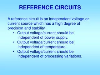
REFERENCE CIRCUITS. A reference circuit is an independent voltage or current source which has a high degree of precision and stability. Output voltage/current should be independent of power supply. Output voltage/current should be independent of temperature.

E N D
REFERENCE CIRCUITS • A reference circuit is an independent voltage or current source which has a high degree of precision and stability. • Output voltage/current should be independent of power supply. • Output voltage/current should be independent of temperature. • Output voltage/current should be independent of process variations. • Bandgap reference circuit widely used, but sill a lot of research improving stability, lowering voltage, reducing area, …
VGS based Current reference MOS version: use VGS to generate a current and then use negative feed back stabilize i in MOS Start up Current mirror VGS
Start up
A widely used Vdd independent Iref generator simple cascoded
Cascode version for low voltage 1/5(W/L)p 1/5(W/L)N K(W/L)N
Sample design steps: • Select Iref (may be given) • Assume all transistors except those arrowed have the same VEB. • VBN = VSS+VTN+VEB; • VBNC = VSS+VTN+VEB*rt(5); • VBP = VDD-|VTP|-VEB; • VBPC = VDD-|VTP|-VEB*rt(5). • At VDDmin, Needs all transistors in saturation. • For PMOS, need VBN < VBPC+|VTP| = VDDmin-VEB*rt(5). VEB < (VDDmin-VSS-VTN)/(1+rt(5)). • For NMOS, need VBP>VBNC-VTN, VDDmin-|VTP|-VEB > VSS+VEB*rt(5). VEB < (VDDmin-VSS-|VTP|)/(1+rt(5)). • Since |VTP| is typically larger, so choose the second one. VEB ≈< (VDDmin-VSS-|VTP|)/(1+rt(5)). • With given VEB and Iref, all (W/L)’s can be determined. • Choose K and R: Iref*R=VEB – VEB/rt(K), so R = (1-1/rt(K))*VEB/Iref. Choose K so that a) R size is not too large and b) R+1/gmn/rt(K) is quite bit larger than 1/gmn.
VEB based current reference Start up VEB=VR
A cascoded version to increase ro and reduce sensitivity: Requires start up Not shown here VEB reference
A thermal voltage based current reference Current mirror I1 = I2, J1 = nJ2, but J = Jsexp(VEB/Vt) J1/J2 = n = exp((VEB1─ VEB2)/Vt) VEB1─ VEB2 = Vt ln(n) I = (VEB1─ VEB2)/R = Vt ln(n)/R Vt = kT/q J2 J1 PTAT
A band gap voltage reference Vout = VEB3 + I*x*R = VEB3 + (kT/q)*xln(n) Vout/T = VEB3/T + (k/q)*xln(n) At room temperature, VEB3/T = ─2.2 mV/oC, k/q = +0.085 mV/oC. Hence, choosing appropriate x and n can make Vout/T=0 When this happens, Vout = 1.26 V
General principle of temperature independent reference Generate a negatively PTAT (Proportional To Absolute Temperature) and a positively PTAT voltages and sum them appropriately.
VBEhas negative temp co at roughly -2.2 mV/°C at room temperature, called CTAT Vt(Vt = kT/q) is PTAT that has a temperature coefficient of +0.085 mV/°C at room temperature. Multiply Vtby a constant K and sum it with the VBEto get VREF = VBE+ KVt If K is right, temperature coefficient can be zero.
VOSrepresents input offset voltage of the amplifier. Transistors Q1 and Q2 are assumed to have emitter-base areas of AE1 and AE2, respectively. If VOSis zero, then the voltage across R1 is given as
In practice, the fabricated value of K (which depends on emitter area ratio, current ratio, and resistance ratio) may not satisfy the given equation. This will lead to Vref value at testing temp to differ from the therretically given value. A resistance value (typically R3) can be then trimmed until Vref is at the correct level. Once this is done, the zero temp co point is set at the testing temperature.
If T0 =300, and T varies by +- 60oC, then Vref changes by as much as 25mV*0.04 = 1 mV. That correspond: 1mV/1.26/120oC = 6.6 ppm/oC In real life, you get about 4X error.
This provides an un-symmetric tilt to the quadratic curve. This provides a faster bending down than the quadratic curve.
A major source of Bdgp error is incorrect calibration. Let T0 be the unkown zero temp co temperature, and Ttest be the test temperature. If Ttest = T0 Else
For example, if Vref is trimmed with an error of 18 mV, this will lead to a slope of 18 mV/300oC at 300oC. In terms of ppm, this is about 50 ppm/oC The actual Vref error due to this trimming error is actually more than this, because the temperature range now is not symmetric about T0.
Causes of errors Vbe2+Vos Vbe2 Vbe1
Converting a bandgap voltage reference to a current reference Trim R1 with intentional error in Vref, so that Vref temp co matches R4 temp co.
Characterization of a bandgap circuit Assuming an ideal op amp with an infinite gain, we have VA = VBand I1 = I2. Schematic of the current-mode bandgap circuit
For the silicon, α=7.021×10⁻⁴V/K, β=1108K, VG(0)=1.17V Since R1=R2, we know IC1 = IC2. Solving for Vbe2: Substituting back
We know I1=IC1+VA/R1. That gives Take partial derivative of I1 with respect to temperature For a given temperature, set the above to 0 and solve for R1. That tells you how to select R1 in terms of temperature, area ratio, and R0. Other quantities are device or process parameters.
In most literature, the last two items are ignored, that allows solution of inflection temperature T0 in terms of R0, R1, area ratio: The current at the inflection point is
Curvature and sensitivity The second-order partial derivative of I1 wrpt T is Notice that under a specific temperature, the second-order derivative is inversely proportional to the resistance R1. We would like to have small variation of I1 around TINF, so it is preferable to have a large R1.
The sensitivity of TINF wrpt R0 and R1 are For R1 = 13.74 KOhm and R0 = 1 KOhm, the sensitivity wrpt R0 is about -6.75, and about 6.5 wrpt R1, when A2/A1 is equal to 8.
Effects of mismatch errors and the finite op amp gain First, suppose current mirror mismatch leads to mismatch between Ic1 and Ic2. In particular, suppose: Re-solve for VA
Finally we get the first line is IC1 and the second is VA/R1 The derivative of I1 wrpt T becomes
Define similar to before: we can calculate