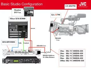
Download

1 / 10
220 likes | 775 Views
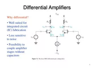
Differential Amplifiers. Why differential? • Well suited for integrated circuit (IC) fabrication • Less sensitive to noise • Possibility to couple amplifier stages without capacitors. Figure 7.1 The basic MOS differential-pair configuration. Operation with a Common-Mode Input Voltage.

E N D
Differential Amplifiers Why differential? • Well suited for integrated circuit (IC) fabrication • Less sensitive to noise • Possibility to couple amplifier stages without capacitors Figure 7.1 The basic MOS differential-pair configuration.
Operation with a Common-Mode Input Voltage Figure 7.2 The MOS differential pair with a common-mode input voltage vCM.
Operation with a Differential Input Voltage Figure 7.4 The MOS differential pair with a differential input signal vid applied. With vid positive: vGS1>vGS2, iD1>iD2, and vD1<vD2; thus (vD2-vD1) will be positive. With vid negative: vGS1<vGS2, iD1<iD2, and vD1>vD2; thus (vD2-vD1) will be negative.
Large-Signal Operation Figure 7.5 The MOSFET differential pair for the purpose of deriving the transfer characteristics, iD1 and iD2 versus vid=vG1 – vG2.
Figure 7.6 Normalized plots of the currents in a MOSFET differential pair. Note that VOV is the overdrive voltage at which Q1 and Q2 operate when conducting drain currents equal to I/2.
Figure 7.7 The linear range of operation of the MOS differential pair can be extended by operating the transistor at a higher value of VOV.
Small-Signal Operation of The MOS Differential Pair Differential Gain Figure 7.8 Small-signal analysis of the MOS differential amplifier: (a) The circuit with a common-mode voltage applied to set the dc bias voltage at the gates and with vid applied in a complementary (or balanced) manner. (b) The circuit prepared for small-signal analysis.
Common-Mode Gain and Common-Mode Rejection Ratio Figure 7.10(a) The MOS differential amplifier with a common-mode input signal vicm. (b) Equivalent circuit for determining the common-mode gain (with ro ignored). Each half of the circuit is known as the “common-mode half-circuit.”
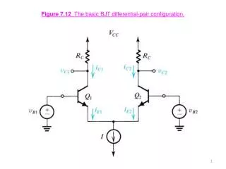
The BJT Differential Pair Figure 7.12 The basic BJT differential-pair configuration.
Figure 7.14 Transfer characteristics of the BJT differential pair of Fig. 7.12 assuming a. 1.