Download
1 / 11
170 likes | 373 Views
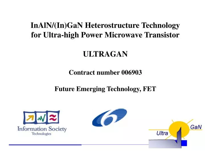
InAlN/(In)GaN Heterostructure Technology for Ultra-high Power Microwave Transistor ULTRAGAN Contract number 006903 Future Emerging Technology, FET. UltraGaN Partnership. 3 Universities: TUW (A), EPFL(CH), TUU(D)

E N D
InAlN/(In)GaN Heterostructure Technology for Ultra-high Power Microwave Transistor ULTRAGAN Contract number 006903 Future Emerging Technology, FET
UltraGaN Partnership 3 Universities: TUW (A), EPFL(CH), TUU(D) 3 public research centres: IEE (Sl), FORTH (Gr), IEMN/CNRS (F), 2 industrial companies: AIXTRON (D), Alcatel-Thales III-V (F)
Applications of GaN-based devices : • Next generation wireless network base stations • Satellite communication systems • Compact digital radar • Scientific and Technical challenge: • Improvements in GaN-based High Electron Mobility Transistors (HEMTs) are limited by the physics of already established AlGaN/GaN heterostructure system • ULTRAGAN project is aiming to explore new heterostructures using InAlN/(In)GaN alloys • The objective is to triple the HEMTs power density if compared to the state-of-the-art large periphery AlGaN/GaN HEMT, meaning almost a factor 50 compared to more classical semiconductors. • InAlN/(In)GaN HEMTs are to demonstrate power densities of 30W/mm at 2 to 12 GHz • The project gives to Europe an opportunity to come back at the edge of the microwave research, which is right now much stronger in the U.S.A.USA and Japan
GaN based heterostructures for HEMT InAlN/GaN: new material, technological difficulties
UltraGaN Progression over the years Initial Target 30 20 10 0 Obtained, Ok with DoW HEMT SiC substrate Higher buffer resistivity AlGaN/GaN InAlN/GaN Heterostructure Validation HEMT Sapphire substrate Year 1 Year 2 Year 3
2008: ULTRAGaN Final Review Report The overall outcome and status of the project is excellent. Given the novelty of the material and the associated problems, both from the material growth as well as the processing and characterization point of view, outstanding progress has been made, resulting in significant contributions to the field of Group-III nitride electronics. From the reviewers point of view, a unique situation appears to have been reached, where a European consortium has achieved a leading role in an area otherwise dominated by US and Japanese research groups. 7 Framework Programme: More robust Gallium Nitride, MORGaN, NMP, IP 214610, 23 partners.
IEE SAS: MOS-HEMTbased on InAlN/GaN InAlN/GaN: High-frequency, high-power devices MOS HEMTbased on InAlN/GaN structure with s Al2O3 insulating layer deposited by MOCVD, Optimisation of preparation and properties
IEE SAS: MOS-HEMTbased on InAlN/GaN Ni/Au S D G 10 nm Al2O3 13,7 nm undoped Al0,82In0,18N 2,1 nm AlN spacer 3 μm GaN buffer Sapphire substrate A 852 Decrease of leakage currents by 3 – 7 orders of magnitude using MOS HEMT approach with MOCVD grown Al2O3 gate insulation
Optimizatin of MOS HEMT preparation Al2O3/InAlN/GaN MOS structures annealed at 700, 800 and 900 oC/2 min in N2 InAlN/GaN: AEC 1559 Alcatel Thales 700 oC 800 oC 900 oC The best performance after 700 oC/2 min anneal