Download
1 / 38
420 likes | 705 Views
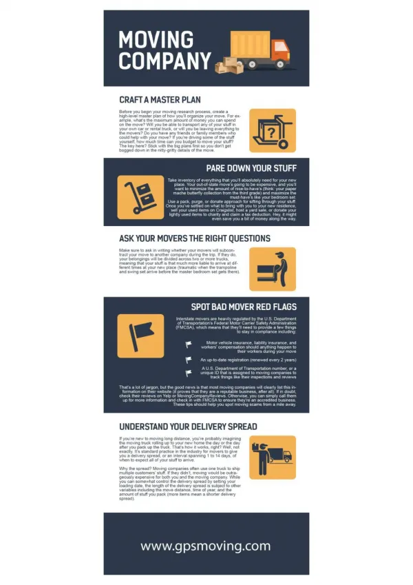
3D IC Technology’s Promise for Communication and Storage ICs. Brian D. Gerson Fellow, VP Research & Development. April 14 th , 2011 Montreal Quebec. Agenda. A Communication and Storage IC perspective on 3D-ICs Cost, power, performance and Time-to-Market (TTM) The promise of 3D-ICs

E N D
3D IC Technology’s Promise for Communication and Storage ICs Brian D. Gerson Fellow, VP Research & Development April 14th, 2011 Montreal Quebec
Agenda • A Communication and Storage IC perspective on 3D-ICs • Cost, power, performance and Time-to-Market (TTM) • The promise of 3D-ICs • Motivation • Defining terms: 2D, 2.5D, 3D devices, and Thru-Silicon-Via (TSV) • State-of-the-art and Roadmaps • Examples of Communication and Storage 3D-ICs • Near, mid, and longer term opportunities • Challenges • Eco-system and CAD Challenges • Summary and Questions
View on 3D ICsA Communication and Storage Semiconductor Perspective “No semiconductor company will adopt 3D ICs because the technology is "cool" (even though it is!)… They'll adopt the technology to make money.” Richard Goering, Technology Journalist • People who have space constraints and are not intimidated by 3D ICs • Right now that equates to the mobile sector -- space can be monetized • The most pressing problems facing the Communication and Storage semi industry today are: developmentcost, power, performance and TTM • For 3D ICs to be relevant to communication and storage semis, it must positively deliver on most if not all of these items! • No way to monetize on the switch to 3D ICs without this…
Rising Development CostCommunication and Storage Perspective Source: IBS and PMC
Total Cost FunctionIt’s all about gate count… • The greatest potential for 3D-IC’s is to increase reuse and decrease TTM while providing enhanced device performance and lower power • 3DC-ICs can’t impact the number of gates only how gates are realized… $Total Cost = $1M +K * (1-Reuse)q *(Unique Gates)r
Gate Power • Below 65nm, static power/Mgate starts to dominate! • How can 3D-IC design help combat the static power challenge? • Better partitioning and process choice of device design Necessary but not sufficient • Use 3D-IC to implement power management features Powerful Power (mW)
High Performance SoC24 and 8 port SAS 2.1, PCIe 3.0 RoCs PM8020 (SRCv 8x6G): • 8 lane SAS-2 controller: 1.5, 3 & 6G SAS/SATA support • 8 lanes of PCI-Express Gen 3 • DDR3-1600MHz memory controller • Wide-port Target Mode • MIPS 1004K processor cluster featuring 2 1 GHz cores • Performance: 250K RAID 0 IOPS • Hardware RAID 0/1/5/50/6/60 acceleration support • On-the-fly RAID Processing Additional PM8015 (SRCv 24x6G): • 24 lane SAS-2 controller: 1.5, 3 & 6G SAS/SATA support • Performance: 300K RAID 0 IOPS • Additional 1GHz processor for increased RAID performance • +60million gate of complex processing, memory, and high-speed mixed signal • Important design considerations • Memory bandwidth and latency • Signal Integrity and mixed-signal performance • IO Per sec (IOPS), measure of device throughput • Power, power, power • How might 3D IC technology positively impact the above?
Agenda • A Communication and Storage IC perspective on 3D-ICs • Cost, power, performance and TTM • The promise of 3D-ICs • Motivation • Defining terms: 2D, 2.5D, 3D, and TSVs • State-of-the-art and Roadmaps • Examples of Communication and Storage 3D-ICs • Near, mid, and longer term opportunities • Challenges • Eco-system and CAD Challenges • Summary and Questions
3D ICs The Promise • 3D-IC design holds the promise of: • Higher bandwidths definite care about • Lower power consumption power is “the new” performance • Increased density interesting but not usually compelling • Lower packaging costs interesting, but skeptical • Benefits of not having to move an entire SoC to an advanced process node Very interesting. HW reuse, lower IC development costs, improved TTM, more value add thru heterogeneous integration • So the potential of 3D ICs positively impacting the Communication and Storage semi space exists…Still some challenges to overcome…More on that later…
Why 3D?Combining Miniaturization and Diversity 3D ICs -- combining Miniaturization with Diversity Source: ITRS Source: of Leti
2DSoCs and SiPs • System-on-Chip (SoC) design costs continue to rise with each technology node • Something has got to give! • System-in-a-Package (SiP) provides heterogeneous integration, but the economics aren’t compelling for most communication and storage semis
2.5DSilicon Interposer • 2.5D device have tremendous potential for Communication and Storage ICs: • Memory, on device DDR and wide IO • Logic partition into higher yield technology node • Heterogeneous RFAMS MEMs devices Source: Shinko
3D More Than Die Stacking • 3D packaging has taken on a definition that is not entirely accurate: that of stacking die. • While die stacking is a portion of what 3D packaging encompasses, its reach extends much further. • Embedded passives and active die into the substrate • Bottom-side die and passive attach • Package-on-package constructions
Early 3D • The idea of 3D-packaging was born from the need to make devices smaller in footprint, yet thinner in profile to meet the challenging form-factor requirements of wireless handsets and portable communications and storage devices • Much of the earlier 3D packaging work revolved around the inexpensive wire-bonding process and package stacking and resulted in many stacked-die and embedded IC solutions • With the advent of flip chip device becoming more and more the norm, the challenge has been how to adopt 3D packaging with flip chip interconnect • TSV is the answer… Source: Signetics Source: Amkor Source: Signetics 8-stack Memory Package-on-Package Package-in-Package
Wafer scale BondingBEOL Fabrication of PIC at Low Temperature • BEOL -Interconnect • Tlimit < 450C, this limits active device fabrication • Excellent isolation of Photonic Passive from Electrical devices • SOTA is III-V to CMOS die bonding • Current research is focused on single XTAL SiGe on amorphous Si Source: Helios Photonic Consortium
Current State-of-the-Artand Roadmap Source: 2010 Electronic and Component Technology Conference John H Lau, ITRI
Agenda • A Communication and Storage IC perspective on 3D-ICs • Cost, power, performance and TTM • The promise of 3D-ICs • Motivation • Defining terms: 2D, 2.5D, 3D, and TSVs • State-of-the-art and Roadmaps • Examples of Communication and Storage 3D-ICs • Near, mid, and longer term opportunities • Challenges • Eco-system and Challenges • Summary and Questions
Integrated Power ManagementImproving Power and Performance thru Integration • Power Management (PM) is not just a system BOM play • Integration of intelligent complete power management solutions • Scalable, small form factor, high performance, system level and managed solutions for complete PM • System power benefits achieved through: • Dynamic voltage scaling based on SOC performance conditions • Adaptive voltage scaling based on process and voltage conditions • Performance achieved through: • High quality regulators and converters to achieve low noise for high performance systems • Power management achieved through 2D • Integrate passives, buck converters, LDOs and control on 2D substrate • Power management integration limited by package substrate area • Power management achieved through 3D • Embedded passives – reduces substrate space and layer count for lower costs • Ball attached die – reduces form factor and substrate area, improves thermal performance 3D provides the opportunity for higher PM integration with higher performance at a lower cost and form factor
BAW and IC Co-integration High-Performance Clocking Achieved thru Packaging Integration • Examples of SiP co-integration of BAW + IC using standard packaging • Thin Film BAW wire-bonded to IC die • Both SiP and Die stacked approaches • Wire-bond approach limited to 7GHz – TSV required to go higher 0.35um CMOS + 1.5-GHz resonator; Digitally-compensated Freq. Reference Source : IEEE Trans. UFFC 2010] 0.13um CMOS + Two 2.1-GHz resonators; FBAR QVCO (left) vs. LC QVCO (right) Source: IEEE JSSC 2008]
Copper Pillar…Highest Impact Advance (in the Near Term)… • Solving I/O pad escape density issues with copper pillar with Bond On Trace (BOT) • Benefits in routing density and EM • Allows very tight bump pitches (<130um) • BOT removes required bump pads and improves density • EM improved to > 150mA • Challenges for adoption • Qualification for ABF (flip-chip) substrates required for very tight routing densities
DDR Memory IntegrationAchieving Capacity Thru Integration • Integrating DDR memories in the same package with Communication and Storage devices is very attractive • SiP approach has only a small positive impact • Small system area savings, some simplified PCB routing, and no significant power saving • Negatively, the costs of the package substrate for the SiP increase due to the addition of the DDR • 3D IC with stack die has a smaller footprint, lower power and potentially lowers costs
Wide I/OAchieving High Performance Memory Low Latency • In Communication and Storage Devices, a common requirement is for low latency, high bandwidth, and random access memory • Current options have area and latency penalties • Wide I/O using TSV technology can address these issues • Implement a low-power wide bus \(~2000 pin) 1600Mb/s interface • Using TSV this interface can be implemented in an area of about 4.3mm^2 assuming 50um signal pitch
2.5D Interposer • In the Communication and Storage space there is a trend to integrate more functions on a device that enable differentiating features • Leads to larger die sizes and/or advanced technology nodes in order to get the die to reasonable die area and costs • Potential savings possible using dual die and quad die approaches with silicon interposer technology • But significant challenges with architecture, partition, and timing! • Heterogeneous integration is the most probable use for Communication and Storage for Interposers Source: PMC Source: EETimes
“Exa-flood” Problem Statement(an Excerpt from G. Astfalk, “Why optical data communications and why now?” Applied Physics A, 2009.) • The rise of “traffic” within data centers is due to increasing numbers of servers, increasing amounts of storage, an increasing number of nodes on the Internet, and increasing backbone traffic • WW growth in servers has a 5-year forward CAGR of 7% • Storage growth has a 5-year forward CAGR of 52% • In 2007, internet traffic is 6.5 exa-bytes per month and the 5-year forward CAGR is 46% • There is a multiplier effect for each byte read or written to disk storage • O(104) bytes of overall communications! • Each byte of traffic traversing the Internet causes perhaps O(106) bytes of data communications within one, or more, data centers! • These place additional stress on the already pressured copper interconnects used throughout current servers and data centers • Copper will continue to struggle with the increased rates while trying to keep power reasonable… • Existing optics solutions can solve the power and speed problems but are expense • Combining Optics with Si processing is predicted to achieve the benefits of Optics while enjoying the cost structure of Si (aka) CMOS manufacturing. • Significant improvements in packaging and fiber attachment required in order for communication and storage device to realize the full potential of optics!
Cu’s Last StandOr how 3D ICs Could Enable Si Photonic XCVRs • Advance modulation schemes (like 16 PAM) and better board materials will move electrical solution to the right • Dropping costs due to Si Photonics solutions will move Optics to the left • 3D ICs will play an important role in achieving lower cost, or reducing $/Gbit Advances in Si Photonics Advances in Modulation
It’s About Power…Performance Metrics for Commercial and Research Links Bit energy per meter versus the maximum reach of the link. Optical links do not include retiming circuitry. Unlike electrical links, the efficiency of the optical link is not sensitive to distance. The potential exists to lower the energy of optical links to < 1pJ/bit at lengths of ~1m. Energy per bit versus maximum reach of the link. Electrical links (blue diamonds) and commercial optical links (red circles) based primarily on VCSELs and CMOS photonic modulators. Source: A. S. Krishnamoorthy, etal, “Progress in Low-Power Switched Optical Interconnect,” IEEE Journal of Selected Topics in Quantum Electronics
Photonic IC Bonding to CMOSMore Complete Transceivers • Flip-chip face-to-face bonding of CMOS device to optical sub-assembly • Enables miniaturization thru a SoC and diversification thru a Photonic IC (PIC) • Enhanced signal integrity due to tight integration between Bi-directional Optical Sub-Assembly BOSA and the SoC • Enables value-add- features (relative to simple BOSA) thru SoC support of the BOSA Source: Helios Photonic Consortium
The Impending ExaFlood • How can we increase the bandwidth of Communication and Storage Devices internal channels to handle the pending Exaflood while dramatically reducing the power per bit required to move data through these channels? • Parallelism has replaced clock frequency scaling • this will work for awhile will only programming as a near term challenge • Eventually (when we’re at 100’s of integrated cores) interconnect performance/power will again halt us at ~ 10fJ/Bit/mm • Optic-Electrical-Optical (O-E-O) systems have the potential to replace conventional electrical high-speed links, internal busses, and data-paths on Communication and Storage Devices • O-E-O systems will be practically realized using advanced 3D IC approaches • Realized first in the move from Petascale to Exascale computing • Subsequently realized in communication and storage Devices as they face the similar challenges as Exascale computing • Performance and power challenge (Energy, Interconnect performance) • Memory and storage challenge (Bandwidth)
3D Exascale DeviceWafer scale Logic, Memory, and Photonics Integration • Each layer separately optimized for performance and yield • Heterogeneous integration that truly combines miniaturization with Diversity • Avoids thermal budget problems associated with fully integrated O-E-O devices • Potentially lower development costs and higher reuse • Promises high-performance with acceptable power • Required to make Exascale devices practical! • Potentially lower system power with l based optical interconnect Wafer-scale 3D integration has the potential to deliver the required improvements in development cost, power, performance and TTM that future Communication and Storage devices need
Cornell Optical RouterExample of Heterogeneous Integration Optical Switching • Phastlane router (right) showing optical and electrical 3D stacked dies, including optical receiver and driver connections to electrical buffers and output multiplexers Source: OSA 2008, N. Sherwood-Droz etal
Agenda • A Communication and Storage IC perspective on 3D-ICs • Cost, power, performance and TTM • The promise of 3D-ICs • Motivation • Defining terms: 2D, 2.5D, 3D, and TSVs • State-of-the-art and Roadmaps • Examples of Communication and Storage 3D-ICs • Near, mid, and longer term opportunities • Challenges • Eco-system and CAD Challenges • Summary and Questions
Developing Eco-systemStandards and Clusters Memory (JC-42) Wide IO (JC-42.6, JC-11) Multi Chip Packaging (JC-63) Qual & Rel (JC-14.3) 3D IC Development & Test Standards 3D IC Enablement IP Standards 3DS-IC Wafer and Tool Standards Bonded Wafer Pair (BWP) * Inspection and Metrology * Thin Wafer Carrier * Single Wafer in Stacked Process 3D Consortium 22 members 3D IC Packaging
CAD Challenges • In order to meet the design challenges of 3D ICs, new tool capabilities are needed in the following areas: • System-level exploration • 3D floor-planning • Implementation (placement, optimization, and routing) • Extraction and analysis • Design for Test (DFT) • IC/package co-design • Mechanical/Stress • Thermal/EMI • Emerging tool chain from a number of CAD vendors • Largely extensions of existing 2D tools • Will require a new breed of “pilots” that are proficient in solving multi-physics problems
Agenda • A Communication and Storage IC perspective on 3D-ICs • Cost, power, performance and TTM • The promise of 3D-ICs • Motivation • Defining terms: 2D, 2.5D, 3D, and TSVs • State-of-the-art and Roadmaps • Examples of Communication and Storage 3D-ICs • Near, mid, and longer term opportunities • Challenges • Eco-system and Challenges • Summary and Questions
Summary • 3D IC offers lots of promise; however, need lots of stuff to be resolved to deliver on that promise • Interposer can be manufactured in volume next 1-2 years • 3D heterogeneous stacks next 3-5 • In the near term, Cu Pillar is very important (its impact perhaps under-rated) • Tools lag is likely to be the pacing item for Industry adoption • Standards will help ease adoption • Opportunities for Communication and Storage devices are: • Near term is power management • Mid-term is silicon interposer wide-I/O • Longer term is heterogeneous integration • Future photonics (ie W2W)