Download

1 / 47
570 likes | 934 Views
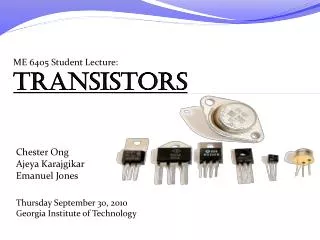
ME 6405 Student Lecture Transistor. Sung-bum Kang Keun Jae Kim Hongchul Sohn Wenwei Xu October 1, 2009 Georgia Institute of Technology. Contents. 1. Introduction to Transistor (Speaker: Sung-bum Kang). 2. Bipolar Junction Transistor (Speaker: Keun Jae Kim). 3. Field Effect Transistor

E N D
ME 6405 Student LectureTransistor Sung-bum Kang Keun Jae Kim Hongchul SohnWenwei Xu October 1, 2009 Georgia Institute of Technology
Contents 1 Introduction to Transistor (Speaker: Sung-bum Kang) 2 Bipolar Junction Transistor (Speaker: Keun Jae Kim) 3 Field Effect Transistor (Speaker: Hongchul Sohn) 4 Power Transistor (Speaker: Wenwei Xu) 5 Applications of Transistor (Speaker: Wenwei Xu)
“Transistor” Part 1 1 Introduction to Transistor (Speaker: Sung-bum Kang) 2 Bipolar Junction Transistor (Speaker: Keun Jae Kim) 3 Field Effect Transistor (Speaker: Hongchul Sohn) 4 Power Transistor (Speaker: Wenwei Xu) 5 Applications of Transistor (Speaker: Wenwei Xu)
Introduction • Question #1: How can we transfer original signal in long distance without loss? • Question #2: How can we control the TV with remote-controller? • Question #3: How can a computer recognize 0(off) and 1(on) for computing? Amplifier and Electronic Switch are needed. • Amplifier: any device that changes, usually increases, the amplitude of a signal. • Electronic Switch: switch that the physical opening and closing is achieved by applying appropriate electrical control signals.
Introduction • However, Vacuum Tube is too big, fragile, and energy-consuming. • Early 20th century, vacuum tube was used for the amplifier and switch. ENIAC, the first general-purpose electronic computer, contains 17,468 vacuum tubes. Vacuum Tube Radio Transistor solved this problem.
Introduction – Invention of Transistor • Invention • In 1947, John Bardeen, Walter Brattain, and William Schockly, researchers at Bell Lab, invented Transistor. • They found Transistor Effect: “when electrical contacts were applied to a crystal of germanium, the output power was larger than the input.” • In 1956, they were awarded the Nobel Prize in physics. • Transistor • is a semiconductor device commonly used to amplify or switch electronic signals. John Bardeen, Walter Brattain, and William Schockly First model of Transistor, 1947
Introduction – Progress of Transistor 1941, Vacuum Tube Edison effect 1948, the first (Germanium) TR John Bardeen, Walter Brattain, and William Schockly 1954, Silicon TR At TI Lab, Ease of processing, lower cost, greater power handling, more stable temperature characteristics 1958, Integrated Circuit Now? Individual electronic components were soldered on to printed circuit boards. IC placed all components in one chip. Sep 2009, 22nm silicon wafer more than 2.9 billion transistors is packed into an area of fingernail Intel CEO Paul Otellini, Sep 23 2009
Introduction – Underlying Science • Semiconductor • is a basic building material of most integrated circuits. • is a material that has an electrical resistivity between that of a conductor and an insulator. • has a few charge carriers(holes or free electrons) and may hence be classified as almost insulator. • However, the conductivity increases by adding impurities(doping). Silicon is used in most commercial semiconductors
Introduction – Underlying Science • Doping • P(positive)-type doping is adding a certain type of atoms to the semiconductor in order to increase holes. • P-type semiconductor, acceptor • N(negative)-type doping is adding some amount of an element with more electrons in order to increase free electrons. • N-type semiconductor, donor Add Group V (Phosphorous) Add Group III(Boron)
Introduction – Underlying Science • PN Junction • is a junction formed by P-type and N-type semiconductors together in very close contact. What happens at the junction? • Electrons(+) from n(-) region diffuse to occupy holes(-) in p(+) region. • Thin depletion region forms near junction.
Introduction – Underlying Science • Forward bias • -V pumps electrons into the N-region. • +V pumps more holes into the P-region. • Excess of charge in P and N region will apply pressure on the depletion region and will make it shrink. • → current flows External Energy • Backward bias • -V sucked out electrons from N-region. • +V sucked out holes from P-region. • The depletion layer widens and it occupies the entire diode(p-n). • → current doesn’t flow
Introduction – Types of Transistor • Transistor are categorized by • Semiconductor material: germanium, silicon, gallium arsenide, etc. • Structure: BJT, FET, IGFET (MOSFET), IGBT • Polarity: NPN, PNP (BJTs); N-channel, P-channel (FETs) • Maximum power rating: low, medium, high • Maximum operating frequency: low, medium, high • Application: switch, audio, high voltage, etc. • Physical packaging: through hole, surface mount, ball grid array, etc. • Amplification factor Various Types of Transistor: http://en.wikipedia.org/wiki/Category:Transistor_types • General Purpose Transistors • Bipolar Junction Transistor (BJT) • Field Effect Transistors (FET) • Power Transistors
“Transistor” Part 2 1 Introduction to Transistor (Speaker: Sung-bum Kang) 2 Bipolar Junction Transistor (Speaker: Keun Jae Kim) 3 Field Effect Transistor (Speaker: Hongchul Sohn) 4 Power Transistor (Speaker: Wenwei Xu) 5 Applications of Transistor (Speaker: Wenwei Xu)
BJT Introduction NPN • 3 Terminals • Base (B) • Collector (C) • Emitter (E) • 2 Types: NPN, PNP • Currents flow in opposite direction • NPN: • BE forward biased • BC reverse biased • PNP: • BE reverse biased • BC forward biased PNP
IC is controlled by IB (Current Control) β (beta) is amplification factor for transistor Typical value of is β 20 ~ 200 BJT Characteristics • iE = iC + iB • iC = βiB • VBE = VB – VE • VCE = VC - VE Georgia Institute of Technology
BJT Operating Regions Operating Regions
BJT Operating Regions Operating Regions
BJT Operating Regions • Cutoff Region: • VBE < Vcut-in, iB = 0 iC = 0, VCE > Vsupply • Active / Linear Region: • VBE = Vcut-in, iB > 0 iC = βiB, Vsat < VCE < Vsupply • Saturation Region: • VBE = Vcut-in, iB > iC,max iC,max, VCE < Vsat Vsupply Vin Georgia Institute of Technology
BJT as Amplifier • Vsupply – iC *RC – VCE=0 Given: • RB = 10 kΩ • RC = 1 kΩ • β= 100 • VSupply = 10 V • Vcut-in= 0.7 V • Vsat = 0.2 V • iC = (Vsupply – VCE) / RC • Set VCE = Vsat = 0.2V • iC = (10 – 0.2) / 1000 = 9.8mA • iC = βiB RC • iB = iC / β = 0.0098/100 = 0.098mA Vin VSupply • Vin - iB*RB– VBE = 0 • Vin = iB*RB + VBE RB • Set VBE = Vcut-in = 0.7V • Vin = 0.098*(10-3)*10000 + 0.7V • Vin = 1.68V or greater. Question: What is the minimum Vin that can use the transistor as an amplifier?
BJT as Switch • From 3rd Exercise • Turns on/off coils digitally
“Transistor” Part 3 1 Introduction to Transistor (Speaker: Sung-bum Kang) 2 Bipolar Junction Transistor (Speaker: Keun Jae Kim) 3 Field Effect Transistor (Speaker: Hongchul Sohn) 4 Power Transistor (Speaker: Wenwei Xu) 5 Applications of Transistor (Speaker: Wenwei Xu)
Field-Effect Transistors • Basics • Conduction of a “channel” is controlled by electric field effect • Very little current flows through input (gate) terminals • Three terminals: gate, source, drain • Voltage-controlled current device control terminal control voltage for charge carriers of charge carriers current channel
Field-Effect Transistors • BJT vs. FET • What was BJT then? • A current-controlled current device • Comparison
Field-Effect Transistors • Types • JFET (Junction FET) • MOSFET (Metal-oxide-semiconductor FET) • MESFET (Metal-semiconductor FET) • HFET (Hetero-structure FET) • MODFET (Modulation doped FET) • IGBT (Insulated-gate bipolar transistor) • Power MOSFETs • FREDFET (Fast reverse or fast recovery epitaxial diode FET) • ISFET (Ion-sensitive FET) • DNAFET • JFET (Junction FET) • MOSFET (Metal-oxide-semiconductor FET)
JFETs • JFETs • n-channel • General Properties • Advantages: Much higher input resistance, lower noise, easier fabrication, ability to handle higher currents and powers • Disadvantages: Slower speeds in switching circuits, smaller bandwidth for a given gain in an amplifier • p-channel
n-channel JFET • Characteristics
n-channel JFET • Characteristics • Idealized Static
n-channel JFET • Characteristics • Practical Static • Transfer
MOSFETs • MOSFETs or Insulated-gate FET (IGFET) • n-channel Enhancement • General Properties • Input resistance even higher • Used primarily in digital electronic circuits • Provide controlled-source characteristics in amplifier circuits • n-channel Depletion
n-channel Enhancement MOSFET • Characteristics
n-channel Enhancement MOSFET • Characteristics • Practical
n-channel Depletion MOSFET • Characteristics • Practical
Applications • Amplifiers, Switches • Task: Design a n-channel common-source JFET Amplifier You CAN do it!! Psst! You can read it!! http://www.electronics-tutorials.ws/amplifier/amp_3.html
“Transistor” Part 4 1 Introduction to Transistor (Speaker: Sung-bum Kang) 2 Bipolar Junction Transistor (Speaker: Keun Jae Kim) 3 Field Effect Transistor (Speaker: Hongchul Sohn) 4 Power Transistor (Speaker: Wenwei Xu) 5 Applications of Transistor (Speaker: Wenwei Xu)
Power Transistor • Concerned with delivering high power • Used in high voltage and high current application • In general • Fabrication process different in order to: • Dissipate more heat • Avoid breakdown • Lower gain than signal level transistor
Power BJT • Same structure to the signal level BJT • The active area is distinctively higher-high current capacity • Thick and low-doped collector region • Large heat dissipation--- larger dimensions
Power MOSFET • Same working principles to MOSFET • Designed to handle large power • Low internal voltage drop and high current capacity • High commutation speed and good efficiency at low voltages—high speed switch
Applications of Transistor building blocks for modern electronics • Digital logic circuits • Microprocessors, microcontrollers, chips (TTL) • Photo-transistors • Replaces normal switches, mechanical relays. • A/D converter • Encoders • Multiplexers • Power supplies wireless communication headphone, microphone microprocessor motor more…
Applications(cont.) • – Switch for a digital signal: BJT or MOSFET • – Switch for a analog signal: JFET • – Switch for a power signal: Power MOSFET or BJT • – Current controlled-current amplifier: BJT • – Voltage controlled-current amplifier: JFET or MOSFET
BJT as switches Small input voltage and large output current operated in the cut-off region(open) and saturation region(close) Example: 2N3904 NPN Assuming LED requires 20-40 mA to provide a bright display and has 2 voltage drop when forwarded biased Output=0V—off Output=5V---on, the transistor is in saturation, with base current Collector current (LED current) is limited by collector resistor
BJT as amplifiers Low input impedance and high voltage gain Audio amplifiers, radio frequency amplifiers, regulated power supplies Example Speaker amplifier BJT series produce higher gain
Applications of FET Advantages of FET over BJT • They are devices controlled by voltage with a very high input impedance (107 to 1012 ohms) • FETs generate a lower noise level than the Bipolar Junction Transistor (BJT) • FETs are more stable than BJT with temperature • FETs are easier to manufacture than the BJT, because they require fewer steps to be built and they allow more integrated devices in the same IC • FETs behave like resistors controlled by voltage for small drain-source voltage values • The high input impedance of FET allows them to withhold loads long enough to allow its usage as storage elements • Power FETs can dissipate higher power and can switch very large currents.
Applications of FET • Amplifiers • Small Signal • Low Distortion • High Gain • Low Noise amplifier • Selectivity • High-Frequency • Switches • Chopper-Type • Analog Gate • Communicator FET Current Limiters Resistors Mixers Oscillators • Protection Diodes • Low-leakage
FET as analog switch-example When VGS = 0, FET becomes saturated and it behaves like a small resistance(<100 ohm)and, therefore, VOUT = {RDS/ (RD + RDS (ON))}* Vin RD>>RDS, VOUT → 0 When a negative voltage equal to VGS (OFF) is applied to the gate, the FET operates in the cut-off region and it acts like a very high resistance usually of some mega ohms. Hence output voltage becomes nearly equal to input voltage.
Contact information(in order of presenting) • Sung-bum Kang sb.kang@gatech.edu • Keun Jae Kim kkim345@gatech.edu • Hongchul Sohn hsohn7@gatech.edu • Wenwei Xu xuw3@gatech.edu
References • www.wikipedia.org • www.google.com • “Introduction to Electrical Engineering”, Mulukata S. Sarma, Oxford University Press, 2001, Chap. 7.4~8.4. • Fall 2008 Transistors Slides • http://www-g.eng.cam.ac.uk/mmg/teaching/linearcircuits/index.html • http://en.wikipedia.org/wiki/FET • http://en.wikipedia.org/wiki/JFET • http://en.wikipedia.org/wiki/MOSFET • http://www.slideshare.net/guest3b5d8a/fets • “Introduction to Electrical Engineering”, Mulukata S. Sarma, Oxford University Press, 2001, Chap. 7.4~8.4. • Fall 2008 Transistors Slides • http://www-g.eng.cam.ac.uk/mmg/teaching/linearcircuits/index.html • http://en.wikipedia.org/wiki/FET • http://en.wikipedia.org/wiki/JFET • http://en.wikipedia.org/wiki/MOSFET • http://www.slideshare.net/guest3b5d8a/fets • http://www.electronics.dit.ie/staff/ypanarin/Lecture%20Notes/K235-1/2%20Transistor-Thyristor.pdf • http://ecee.colorado.edu/~bart/book/book/chapter5/ch5_9.htm • http://www.ece.mtu.edu/labs/EElabs/EE3305/Bipolar_Junction_Transistors.pdf • http://www.partminer.com/glossaryhtml/bjt.htm • http://www.lycos.com/info/bipolar-junction-transistor--applications.html • http://jimwarholic.com/uploaded_images/power-supply-768753.jpg • http://abbydamico.files.wordpress.com/2008/09/microprocessor-athlon-64.jpg • http://www.billfrymire.com/blog/wp-content/uploads/2008/05/wireless-communication-connection-1000.jpg • http://www.cybermediatech.com/images/WirelessHeadphone-big.jpg • http://www.colorado.edu/physics/phys3330/phys3330_fa09/pdfdocs/AN101FETintro.pdf • http://www.circuitstoday.com/fet-applications
Thank you! Questions?