Download
1 / 14
140 likes | 239 Views
Projects at the MPI Semiconductor laboratory: DEPFETs and 3D integration. Two R&D projects which might be interesting for this meeting DEPFET monolithic pixel sensor Precision vertex detector (ILC and SuperBelle) X-ray imaging

E N D
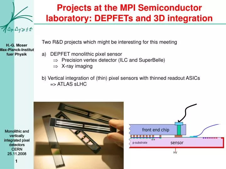
Projects at the MPI Semiconductor laboratory: DEPFETs and 3D integration • Two R&D projects which might be interesting for this meeting • DEPFET monolithic pixel sensor • Precision vertex detector (ILC and SuperBelle) • X-ray imaging • b) Vertical integration of (thin) pixel sensors with thinned readout ASICs • => ATLAS sLHC
Active Pixel Sensors • Integrate sensor (diode) and readout electronics in one device • Reduce material • Reduce interconnection capacitance (better S/N) • Reduce cost (fine pitch bump bonding: 300$/cm2) • Conflicting requirements: • Sensors CMOS electronics • Bulk silicon high resistivity low resistivity • Wafer 4” – 6” 8” and larger • Oxide thick thin • Etching wet dry (RIE) • Feature size >1 mm <0.25 mm (getting smaller) • Lithography Proximity Projective • Device size wafer reticle (cm2) • Options: MAPS/SOI (CMOS technology) • DEPFET (Sensor technology) • 3D integration: both
DEPFET • Each pixel is a p-channel FET on a completely depleted bulk • A deep n-implant creates a potential minimum for electrons under the gate (“internal gate”) • Signal electrons accumulate in the internal gate and modulate the transistor current (gq ~ 400 pA/e-) • Accumulated charge can be removed by a clear contact (“reset”) • Rolling shutter mode (column parallel) for matrix operation • Fully depleted: • large signal, fast signal collection • Low capacitance, • internal amplification: => low noise
Performance Fe55: 1.6 e- rms noise, Room temperature ! 10 ms shaping time Low noise: x-ray spectroscopy and imaging High speed -> noise ~ t-1/2 At 50MHz: ENC < 40e (=> 50ns line rate! ) For tracking: even thinned (but fully depleted) detectors have excellent S/N S/N > 140 measured for d=450 mm S/N ~ 40 achievable for d=50 mm Position resolution < 2 mm in beam tests
Projects: Particle Physics Large S/N even for thin sensors with high readout bandwidth Thinning technology to produce thin large (10 cm) monolithic all silicon sensors without need of extra support material • X0 ~ 0.1% achievable • Sufficient radiation hard O(10 MRad) • Precision vertex detectors at e+e- colliders • ILC • SuperBelle Barcelona, Bonn, Cracow, Giessen, Goettingen, Heidelberg, Karlsruhe, Munich, Prague, Santander, Santiago de Compostela, Vienna, Valencia
7.1 cm 8.4 cm SuperBelle • KEKB upgrade to reach 8x1035 cm-2s-1 • High occupancy: 0.4 hits/mm2/s • Radiation: 1MRad/year • Low momentumm tracks: thin sensors • Schedule for 2013 2 layer pixel detector 1.3/1.8 cm radius (?) 20-24 modules Pixel: 50 x 75 mm2 256 x 1000 pixel 100 kHz Frame rate (10 ms/frame) 50 mm thick sensor ~ 0.15% X0 >1 Gbit/s per module
X-ray Imaging • X-ray astronomy • excellent focal plane detector • -efficient up to 20 keV • Low noise: < 2 e- • Fast readout • No deadtime (unlike CCDs) • No cooling needed • XEUS/IXO • BepiColombo • Simbol-X 8 bits 0.78mV x 256 7 bits 0.78mV x 128 XFEL (free electron laser) 5 MHz frame readout 1024 x 1024 pixels => Non linear response Single photon resolution at 1 keV Dynamic range: 6000 photons (1keV)
50 mm 400 mm 3D integration for HEP detectors Multilayer electronics: Split analogue and digital part Use different, individually optimized technologies: -> gain in performance, power, speed, rad-hardness, complexity. -> smaller area (reduce pixel size or more functionality). 4-side abuttable devices: -> no dead space. -> simpler module layout. -> larger modules. (reduce complexity and material) 50 x 400 mm2 (0.25 mm) May shrink to ~ 50 x 50 mm2 (130 nm) 50 mm 50 mm Periphery, column logic, services Pixel area
MPI 3D R&D Program • Build demonstrator using ATLAS pixel chip (FE-I2/3) and thin pixel sensors made by MPI • Use SLID and ICV technology by Fraunhofer IZM • R&D Issues: • Technology: compatible with sensors, ASICs? • Interconnection quality: e.g. capacitance (face-to-face or die up?). • Yield & Costs. • Production in industry. • Reduce material (copper layer).
IZM SLID Process • Alternative to bump bonding (less process steps “low cost” (IZM)). • Small pitch possible (<< 20 mm, depending on pick & place precision). • Stacking possible (next bonding process does not affect previous bond). • Wafer to wafer and chip to wafer possible.
Through Silicon Vias • Hole etching and chip thinning • Via formation with W-plugs. • Face to face or die up connections. • 2.5 Ohm/per via (including SLID). • No significant impact on chip performance • (MOS transistors). ICV = Inter Chip Vias
Tests on Diodes at IZM • Diode Test wafers processed at IZM • Preparation for SLID process • Diffusion barriers & Cu layers • Thermal treatment • Diode properties unchanged
SLID Pad 27x360 mm2 50% SLIDcoverage SLID Pad 27x58 mm2 10% SLID coverage Al BCB 25 um 20 um Cu3Sn 30 um 15 um Al SiO2 Tests on metal dummies at IZM Test of “chip on wafer” SLID interconnection with metal dummies. • Aim: determine the feasibility of the SLID inter-connection within the parameters we need for the ATLAS pixels. • Test of the mechanical strength as a function of different area coverage by the SLID pads • Test the SLID efficiency varying the dimensions of the SLID pads • Study the SLID efficiency when degrading the planarity of the structure underneath the pads • Determine the alignment precision between single “chip” and “detector” wafer • Investigate the BCB isolation capability between the detector and chip surfaces • Currently processed at IZM, expected back before x-mas
Summary MPI Semiconductor laboratory has 2 R&D projects for highly integrated pixel detectors DEPFET: monolithic pixel sensor with integrated amplification one FET amplifier/pixel fully depleted low noise high readout speed wafer scale, thinned devices ILC, SuperBelle, X-ray astronomy, XFEL Vertical (“3D”) integration of pixel sensors (diodes) and ASICs high density, low cost interconnect (SLID) four side buttable devices (through silicon vias) optimize sensor technology for 3D interconnection! sLHC, (XFEL) Plans to use 3D version of ATLAS FE-I4 pixel chip later (Orsay activity with Fermilab/Tezzaron))