Download
1 / 1
10 likes | 131 Views
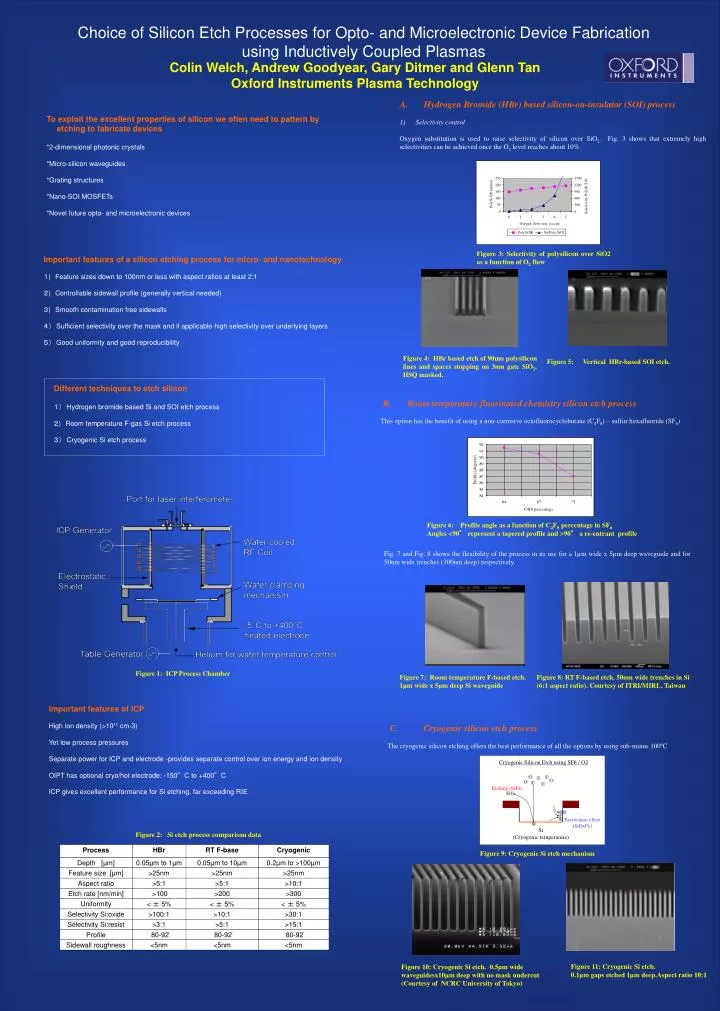
Cryogenic Silicon Etch using SF6 / O2. O. F. F. O. O. F. F. Etching (SiFx). Si. F. O. Si. F. Passivation effect (SiOxFy). Si. Si. Si (Cryogenic temperature). Choice of Silicon Etch Processes for Opto- and Microelectronic Device Fabrication using Inductively Coupled Plasmas.

E N D
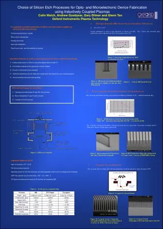
Cryogenic Silicon Etch using SF6 / O2 O F F O O F F Etching (SiFx) Si F O Si F Passivation effect (SiOxFy) Si Si Si (Cryogenic temperature) Choice of Silicon Etch Processes for Opto- and Microelectronic Device Fabrication using Inductively Coupled Plasmas Colin Welch, Andrew Goodyear, Gary Ditmer and Glenn Tan Oxford Instruments Plasma Technology A. Hydrogen Bromide (HBr) based silicon-on-insulator (SOI) process 1) Selectivity control Oxygen substitution is used to raise selectivity of silicon over SiO2. Fig. 3 shows that extremely high selectivities can be achieved once the O2 level reaches about 10%. To exploit the excellent properties of silicon we often need to pattern by etching to fabricate devices *2-dimensional photonic crystals *Micro-silicon waveguides *Grating structures *Nano-SOI MOSFETs *Novel future opto- and microelectronic devices Important features of a silicon etching process for micro- and nanotechnology 1)Feature sizes down to 100nm or less with aspect ratios at least 2:1 2)Controllable sidewall profile (generally vertical needed) 3)Smooth contamination free sidewalls 4) Sufficient selectivity over the mask and if applicable high selectivity over underlying layers 5) Good uniformity and good reproducibility Figure 3: Selectivity of polysilicon over SiO2 as a function of O2 flow Figure 4: HBr based etch of 90nm polysilicon lines and spaces stopping on 3nm gate SiO2. HSQ masked. Figure 5:Vertical HBr-based SOI etch. Different techniques to etch silicon 1) Hydrogen bromide based Si and SOI etch process 2) Room temperature F-gas Si etch process 3) Cryogenic Si etch process B. Room temperature fluorinated chemistry silicon etch process This option has the benefit of using a non-corrosive octofluorocyclobutane (C4F8) – sulfur hexafluoride (SF6) Figure 6: Profile angle as a function of C4F8 percentage in SF6 Angles <90° represent a tapered profile and >90° a re-entrant profile Fig. 7 and Fig. 8 shows the flexibility of the process in its use for a 1µm wide x 5µm deep waveguide and for 50nm wide trenches (300nm deep) respectively. Figure 1: ICP Process Chamber Figure 7: Room temperature F-based etch. 1µm wide x 5µm deep Si waveguide Figure 8: RT F-based etch. 50nm wide trenches in Si (6:1 aspect ratio). Courtesy of ITRI/MIRL, Taiwan Important features of ICP High ion density (>1011 cm-3) Yet low process pressures Separate power for ICP and electrode -provides separate control over ion energy and ion density OIPT has optional cryo/hot electrode: -150°C to +400°C ICP gives excellent performance for Si etching, far exceeding RIE C. Cryogenic silicon etch process The cryogenic silicon etching offers the best performance of all the options by using sub-minus 100ºC Figure 2: Si etch process comparison data Figure 9: Cryogenic Si etch mechanism Figure 11: Cryogenic Si etch. 0.1µm gaps etched 1µm deep.Aspect ratio 10:1 Figure 10: Cryogenic Si etch. 0.5µm wide waveguidesx10µm deep with no mask undercut (Courtesy of NCRC University of Tokyo)