Download
1 / 30
300 likes | 414 Views
Design of a Power-Efficient Interleaved CIC Architecture for Software Defined Radio Receivers. By J.Luis Tecpanecatl-Xihuitl, Ruth Aguilar-Ponce, Ashok Kumar, Magdy A. Bayoumi. Center for Advanced Computer Studies (CACS) University of Louisiana at Lafayette Lafayette, LA, USA. Outline.

E N D
Design of a Power-Efficient Interleaved CIC Architecture for Software Defined Radio Receivers By J.Luis Tecpanecatl-Xihuitl, Ruth Aguilar-Ponce, Ashok Kumar, Magdy A. Bayoumi Center for Advanced Computer Studies (CACS) University of Louisiana at Lafayette Lafayette, LA, USA
Outline • Introduction • Goal • Cascaded-Integrator-Comb (CIC) Filter • Proposed Architecture • Results • Conclusions
Introduction • Two important current factors targeting Circuits for Communications: • High Data Rates • Multistandard Devices * Topics in Circuits for Communications IEEE Communications Magazine, August 2005
Introduction • High Data Rates • Much information in is being to transferred between many of these devices • PVR to flat- screen may require 221-1327 Mb/s. • Downloading 1000 songs from a media center or Pc to MP3 player require 200 Mb/s in a reasonable amount of time. * Topics in Circuits for Communications IEEE Communications Magazine, August 2005
Multistandard Devices • Portable devices integrating not only camera and cellphone, but also WLAN. • Personal Video Recorder (PVR), Gaming and Digital TV. • At the same time dissipating low power for long battery lifetime.
Introduction • Use of Multi-Standard Digital Receiver • Transition between generations • 2G 3G 4G • 4G “ABC” Always Be Connected • Data Networks, PCS, Bluetooth, and more
Data Nets Next Generation 4G Old Standards Specific Standard 3G PCS Nets 2G Introduction
Introduction • Several Communication Standards • Incompatibility between them • For Example GSM in USA vs. Europe • Many devices per user • High Cost of new infrastructure
Introduction • Benefits of Multi-Standard Device • Several Standards • Take advantage of current infrastructure • Take advantage of different service providers • Configurable by a PC, same provider or by itself
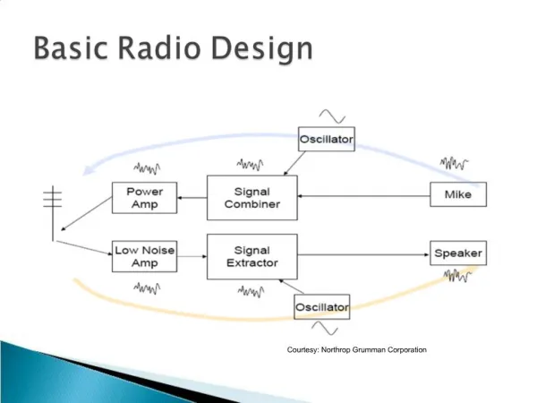
Analog Digital Anti-aliasing Filter ADC DSP LNA Introduction • How can this be possible? • Software-defined Radio • Implement the different functionalities of a transceiver by means of software • Flexibility
Digital NCO Multistage Decimation Filters Analog I R H(z) Anti-aliasing Filter ADC LNA Q H(z) R NCO Introduction • Architecture • Going so close to the antenna
Introduction • Digital Down Converter • Analog-to-Digital Converter (ADC) • Numerical Control Oscillator (NCO) • Mixers (Multipliers) • Decimator Filter • Frequency translation • Computational intensive • Power demanding
accelerators ADC DAC DSP Introduction • Accelerator • Dedicated pieces of hardware which are not programmable • Low power consumption • Reduced Area • Flexibility
X(ej) 2 0 1 H(ej) 0 /M 2 H(z) M Fin W(ej) Fout = Fin/M 0 /M Y(ej’) 0 8/M 2/M 4/M /M 6/M 0 ’ 4 8 2 6 Introduction • Decimator • Digital Filter • Downsampler If M >> 2 then Coefficient length of H(z) Increase CIC good candidate
Introduction • Distribution of power consumption on a Tap (multiplication, addition) • Multiplication: 40% to 76% of total power consumption on each tap • Additions: 14% to 25% of total power consumption on each tap Tap Filter Multiplication, Addition and Delay
Major sources of power dissipation in digital CMOS circuits • Switching • Short-circuit • Leakage currents Ptotal = pt(CL V Vddfclk ) + IscVdd + IleakageVdd
1.-System 2.-Algorithm 3.-Architecture 4.-Logic/Circuit 5.-Device/Process Introduction • Process Design • Identification of the blocks or parts consuming an important fraction of the power during optimization process.
Goal • Power Reduction on CIC Filter • Reduced frequency of operation • Voltage Scaling • One structure to filter both Signals • Interleaving 3. Common Structure for different communication standards
Integrator M Comb fs fs /M M z-1 z-1 z-1 z-1 k stages k stages CIC Filter • Cascaded Integrator-Comb Filter • Advantages • Multiplierless implementation • No memory storage 39 bits 19 bits Wide wordlength
I CIC Multistage Filters I ADC CIC Q Q Integrator M Comb fs fs /M CIC Filter • Two CIC filters • Double area • Power consumption • Integrator Section • Frequency input • Wide Wordlength
Proposed Architecture • Polyphase filter operates at frequency f/R1, where f is the input frequency. • The polyphase filter structure for decimation filtering helps to reduce the speed requirement grouping the filter in subfilters. The serial input is passed to be filter by the subfilters. The outputs are added to obtain the final output. Thus, the subfilters will operate at reduced frequency fs/D, where D is the factor of decimation
Proposed Architecture • The dynamic power dissipation in digital CMOS circuits can be modeled as • The polyphase architecture is composed of polyphase components operating at the rate of f/M. Therefore, in these polyphase components, it is possible to reduce the voltage supply, which has an important impact on the power consumption. V’dd can be approximated by
Proposed Architecture • Voltage Scaling • The obtained scaled voltage supply causes no degradation in the performance of the whole structure. For the stages after the polyphase CIC filter the same voltage supply scaled is used without no decrement effect on performance because the sampling rate is reduce each time.
Results • Wordlengths on CIC filter
Results • Power estimation • Three different factors • For our estimation, adders are the major power consumer blocks for the direct CIC filter in the new architecture due to their dominant capacitance
Results • where P0 denoted the power consumption of the reference system. The previous estimations correspond to the three different decompositions showed in previous Table. • Therefore, the power consumption of the Interleaved CIC polyphase architecture is only around 15% of the original system.
Results • Frequency Response • Interleaved CIC polyphase structure is simulated in MATLAB
Conclusions • Combination of different methods has been adopted to reduce the power consumption on CIC filters used on multistandard digital receivers implemented as software defined radio. • Interleaving both signals I and Q, in a polyphase architecture results in a more efficient structure which works at low frequency.
Conclusions • On each polyphase component the voltage supply is scaled to reduce the power consumption without compromising the performance of the whole architecture. • The power consumption in the proposed architecture is estimated to be approximately 15% of the common architecture on the three cases.