Download

1 / 54
540 likes | 895 Views
Mini-MIPS. From Weste/Harris CMOS VLSI Design. Based on MIPS. In fact, it’s based on the multi-cycle MIPS from Patterson and Hennessy Your CS/EE 3810 book... 8-bit version 8-bit data and address 32-bit instruction format 8 registers numbered $0-$7 $0 is hardwired to the value 0.

E N D
Mini-MIPS From Weste/Harris CMOS VLSI Design
Based on MIPS • In fact, it’s based on the multi-cycle MIPS from Patterson and Hennessy • Your CS/EE 3810 book... • 8-bit version • 8-bit data and address • 32-bit instruction format • 8 registers numbered $0-$7 • $0 is hardwired to the value 0
Fibonacci C-Code Cycle 1: f1 = 1 + (-1) = 0, f2 = 0 – (-1) = 1 Cycle 2: f1 = 0 + 1 = 1, f2 = 1 – 1 = 0 Cycle 3: f1 = 1 + 0 = 1, f2 = 1 – 0 = 1 Cycle 4: f1 = 1 + 1 = 2, f2 = 2 – 1 = 1 Cycle 5: f1 = 2 + 1 = 3, f2 = 3 – 1 = 2 Cycle 6: f1 = 3 + 2 = 5, f2 = 5 – 2 = 3
Fibonacci Assembly Code Compute 8th Fibonacci number (8’d13 or 8’h0D) Store that number in memory location 255
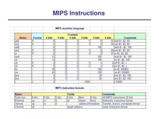
Fibonacci Machine Code 4 101000 Machine Code Assembly Code
External Memory from Book // external memory accessed by MIPS module exmemory #(parameter WIDTH = 8) (input clk, input memwrite, input [WIDTH-1:0] adr, writedata, output reg [WIDTH-1:0] memdata); reg [31:0] RAM [(1<<WIDTH-2)-1:0]; wire [31:0] word; // Initialize memory with programinitial $readmemh("memfile.dat",RAM); // read and write bytes from 32-bit word always @(posedge clk) if(memwrite) case (adr[1:0]) 2'b00: RAM[adr>>2][7:0] <= writedata; 2'b01: RAM[adr>>2][15:8] <= writedata; 2'b10: RAM[adr>>2][23:16] <= writedata; 2'b11: RAM[adr>>2][31:24] <= writedata; endcase assign word = RAM[adr>>2]; always @(*) case (adr[1:0]) 2'b00: memdata <= word[7:0]; 2'b01: memdata <= word[15:8]; 2'b10: memdata <= word[23:16]; 2'b11: memdata <= word[31:24]; endcase endmodule • Notes: • Endianess is fixed here • Writes are on posedge clk • Reads are asynchronous • This is a 32-bit wide RAM • With 64 locations • But with an 8-bit interface...
Exmem.v module exmem #(parameter WIDTH = 8, RAM_ADDR_BITS = 8) (input clk, en, input memwrite, input [RAM_ADDR_BITS-1:0] adr, input [WIDTH-1:0] writedata, output reg [WIDTH-1:0] memdata); reg [WIDTH-1:0] mips_ram [(2**RAM_ADDR_BITS)-1:0]; initial $readmemb("fib.dat", mips_ram); always @(posedge clk) if (en) begin if (memwrite) mips_ram[adr] <= writedata; memdata <= mips_ram[adr]; end endmodule • This is synthesized to • a Block RAM on the • Spartan3e FPGA • It’s 8-bits wide • With 256 locations • Both writes and reads are clocked
Exmem.v module exmem #(parameter WIDTH = 8, RAM_ADDR_BITS = 8) (input clk, en, input memwrite, input [RAM_ADDR_BITS-1:0] adr, input [WIDTH-1:0] writedata, output reg [WIDTH-1:0] memdata); reg [WIDTH-1:0] mips_ram [(2**RAM_ADDR_BITS)-1:0]; initial $readmemb("fib.dat", mips_ram); always @(posedge clk) if (en) begin if (memwrite) mips_ram[adr] <= writedata; memdata <= mips_ram[adr]; end endmodule This is synthesized to a Block RAM on the Spartan3e FPGA Note clock!
Block RAM Byte-wide Block RAM is really 9-bits – parity bit... (Actually dual ported too!)
Our Block Ram • Read-first or Write-first? always @(posedge clk) if (en) begin if (memwrite) mips_ram[adr] <= writedata; memdata <= mips_ram[adr]; end
Block RAM Organization Block RAM is Single or Dual ported Each block is 18k bits...
Recall – Overall System Clock Clk Clk
Recall – Overall System Clock Clk Clk So, what are the implications of using a RAM that has both clocked reads and writes instead of clocked writes and async reads? (we’ll come back to this question...)
mips.v // simplified MIPS processor module mips #(parameter WIDTH = 8, REGBITS = 3) (input clk, reset, input [WIDTH-1:0] memdata, output memread, memwrite, output [WIDTH-1:0] adr, writedata); wire [31:0] instr; wire zero, alusrca, memtoreg, iord, pcen, regwrite, regdst; wire [1:0] aluop,pcsource,alusrcb; wire [3:0] irwrite; wire [2:0] alucont; controller cont(clk, reset, instr[31:26], zero, memread, memwrite, alusrca, memtoreg, iord, pcen, regwrite, regdst, pcsource, alusrcb, aluop, irwrite); alucontrol ac(aluop, instr[5:0], alucont); datapath #(WIDTH, REGBITS) dp(clk, reset, memdata, alusrca, memtoreg, iord, pcen, regwrite, regdst, pcsource, alusrcb, irwrite, alucont, zero, instr, adr, writedata); endmodule
Controller State Codes Useful constants to compare against State Register
Output Logic Very common way to deal with default values in combinational Always blocks Continued for the other states...
Output Logic Two places to update the PC pcwrite on jump pcwritecond on BEQ Why AND these two?
ALU Invert b if subtract... add is a + b sub is a + ~b +1 subtract on slt then check if answer is negative
Register File What is this synthesized into?
Synthesis Report Two register files? Why?
Datapath Fairly complex... Not really, but it does have lots of registers instantiated directly It also instantiates muxes... Instruction Register
Datapath continued RF and ALU Flops and muxes...
Back to the Memory Question • What are the implications of using RAM that is clocked on both write and read? • Book version was async read • So, let’s look at the sequence of events that happen to read the instruction • Four steps – read four bytes and put them in four slots in the 32-bit instruction register (IR)
Instruction Fetch • Memread, irwrite, addr, etc are set up just after clk edge • Data comes back sometime after that (async) • Data is captured in ir0 – ir3 on the next rising clk edge • How does this change if reads are clocked?
mips + exmem mips is expecting async reads exmem has clocked reads One of those rare cases where using both edges of the clock is useful!
Memory Mapped I/O • Break memory space into pieces (ranges) • For some of those pieces: regular memory • For some of those pieces: I/O • That is, reading from an address in that range results in getting data from an I/O device • Writing to an address in that range results in data going to an I/O device
Mini-MIPS Memory Map FF 8-bit addresses 256 bytes total! 1111 1111 I/O Switches/LEDs 1100 0000 C0 BF Code/Data 1011 1111 1000 0000 80 Top two address bits define regions Code/Data 0111 1111 7F 0100 0000 40 0011 1111 3F Code/Data 64 bytes 0000 0000 00
Enabled Devices Only write to that device (i.e. enable it) if you’re in the appropriate memory range. Check top two address bits!