Download
1 / 2
20 likes | 127 Views
Coupling between Piezoelectricity and Charge Transport Property in ZnO Nanowires Xudong Wang, University of Wisconsin-Madison, DMR 0905914.

E N D
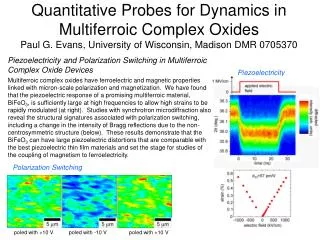
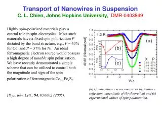
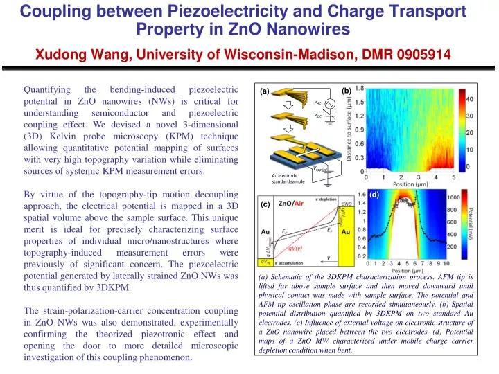
Coupling between Piezoelectricity and Charge Transport Property in ZnO Nanowires Xudong Wang, University of Wisconsin-Madison, DMR 0905914 Quantifying the bending-induced piezoelectric potential in ZnO nanowires (NWs) is critical for understanding semiconductor and piezoelectric coupling effect. We devised a novel 3-dimensional (3D) Kelvin probe microscopy (KPM) technique allowing quantitative potential mapping of surfaces with very high topography variation while eliminating sources of systemic KPM measurement errors. By virtue of the topography-tip motion decoupling approach, the electrical potential is mapped in a 3D spatial volume above the sample surface. This unique merit is ideal for precisely characterizing surface properties of individual micro/nanostructures where topography-induced measurement errors were previously of significant concern. The piezoelectric potential generated by laterally strained ZnO NWs was thus quantified by 3DKPM. The strain-polarization-carrier concentration coupling in ZnO NWs was also demonstrated, experimentally confirming the theorized piezotronic effect and opening the door to more detailed microscopic investigation of this coupling phenomenon. (b) (a) (d) (c) (a) Schematic of the 3DKPM characterization process. AFM tip is lifted far above sample surface and then moved downward until physical contact was made with sample surface. The potential and AFM tip oscillation phase are recorded simultaneously. (b) Spatial potential distribution quantified by 3DKPM on two standard Au electrodes. (c) Influence of external voltage on electronic structure of a ZnO nanowire placed between the two electrodes. (d) Potential maps of a ZnO MW characterized under mobile charge carrier depletion condition when bent.
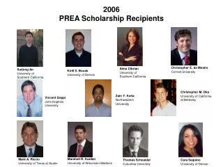
Coupling between Piezoelectricity and Charge Transport Property in ZnO Nanowires Xudong Wang, University of Wisconsin-Madison, DMR 0905914 Through the collaboration with UW Research Experiences for Teachers (RET) program, we hosted a high school teacher (Lori Brooks) from Beaver Dam, WI for an intensive six-week, full-time, research experience development. We designed a project for her high school chemistry classes using TiO2 nanoparticles for photo-degeneration of water pollutants. She learned the fundamentals of photovoltaic and photoelectrochemistry. She successfully demonstrated a UV-induced electrochemical reaction for organic degeneration. We also helped her to improve this experiment to a larger-scale setup for teaching high school students. A high school teacher is practicing photo-degeneration reactions of water pollutants and explaining the mechanisms to her students.