Download
1 / 5
50 likes | 54 Views
Ampere VLSI Academy, a division of Mobiveil Technologies, offers a high-profile VLSI Verification course in the field of Semiconductor design. Ampere VLSI Academy, a division of Mobiveil Technologies, has structured the course to have right mix of lectures combined with lab projects to transform a graduate engineer to a skilled work force in Verification domain which is on demand today across the globe. http://www.amperevlsi.com/

E N D
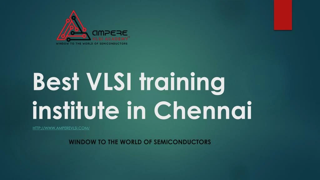
Best VLSI training institute in Chennai http://www.amperevlsi.com/ window to the world of semiconductors
Designing a VLSI IC http://www.amperevlsi.com/ • The process includes designing, starting from gates to design for testability. Backend design comprises of CMOS library design and its characterization. It also covers physical design and fault simulation. The entire design procedure follows a step by step approachProblem Specification • It is a high-level representation of the system. The major parameters are performance, functionality, physical dimensions, fabrication technology and design techniques. It has to be a tradeoff between market requirements, the available technology and the economic viability of the design.
Architecture DefinitionBasic specifications like floating point units, which system to use, like reduced instruction set computer (RISC) or complex instruction set computer (CISC), number of ALU’s cache size etc. Functional Design Defines the major functional units of the system and hence facilitates the identification of interconnect requirements between units, the physical and electrical specifications of each unit. Logic Design Boolean expressions, control flow, word width, register allocation etc. are developed and the outcome are the register transfer level (RTL) description. HDLs implement the RTL description onto a system.
Circuit DesignWhile the logic design gives the simplified implementation of the logic,the realization of the circuit in the form of a netlist is done in this step. The netlist consists of gates, transistors and various interconnects. This again is a software step and the outcome is checked via simulation. Physical Design • The conversion of the netlist into its geometrical representation is done in this step and the result is called a layout. This step follows some predefined fixed rules like the lambda rules which provide the exact details of the size, ratio and spacing between components. Etching • It removes material selectively from the surface of wafer to create patterns. An etching mask protects some parts of the material. Additional chemicals or plasma removes the remaining photoresist. An inspection makes sure the transference of the image from mask to the top layer of wafer.
amperevlsi ADRESS: EMM YES PARK, 2nd floor, Jawaharlal Nehru Road, Ekkattuthangal, Chennai – 600032. PHONE NUMBER: 7338852862 EMAIL: enroll@amperevlsi.com WEBSITE: http://www.amperevlsi.com/