Download
1 / 1
10 likes | 168 Views
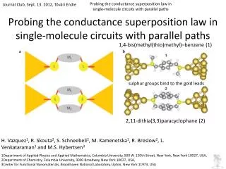
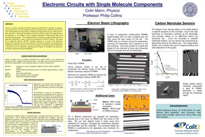
PMMA / SiO 2. SWCNT. On. Off. S ummer U ndergraduate 2 R esearch 0 F ellowship in 0 I nformation 6 T echnology. Electron Beam Lithography. Carbon Nanotube Sensors. Electronic Circuits with Single Molecule Components. ABSTRACT

E N D
PMMA / SiO2 SWCNT On Off S ummer U ndergraduate 2R esearch 0F ellowship in 0I nformation6T echnology Electron Beam Lithography Carbon Nanotube Sensors Electronic Circuits with Single Molecule Components ABSTRACT The use of carbon nanotube field-effect transistors (CNTFETs) as chemical or biological sensors is the focus of many research groups in nanotechnology. CNTFET sensors have been demonstrated with extraordinary sensitivities ranging from parts per million down to parts per trillion. These high sensitivities could allow a broad range of new applications in the detection of, for example, toxins, regulated substances, industrial gas leaks, and chemical warfare agents . The immediate goal of this project is to fabricate devices with a particular architecture in order to study the mechanisms of CNTFET sensors. We would like to determine whether CNTFET chemical response is a result of the interaction between the nanotube and the test chemical or the junction between the nanotube and electrodes and the test chemical. My role in the project is centered around the fabrication of devices for such an experiment, specifically, the creation of “windows” over portions of nanotubes using electron beam lithography. The design of our devices allows us to create defects in specific locations on the nanotube. Due to the high sensitivity of nanotubes, covering up the electrodes and contacts allows us to determine where the sensitivity lies. Once the nanotube is oxidized (eletrically broken), we can recover the conductivity by depositing metal at the defect site. The image below shows such a defect site and it’s response before and after deposition on the graph. A layer of polymethyl methacrylate (PMMA) approximately 200 nm thick is placed over the chip using the spin coater on the left. The PMMA acts as a barrier during the experiment, covering the electrodes from exposure to the test chemical. Once the window is in place this allows for the chemical to have sole interaction with the nanotube and not the electrodes. SEM Spin Coater CARBON NANOTUBE BACKGROUND Carbon nanotubes are an ordered arrangement of carbon atoms in two dimensional hexagonal arrays, wrapped into seamless tubes. This gives rise to unique electronic and mechanical characteristics. Some important aspects of carbon nanotubes are: Structure : analogous to a layer of graphite wrapped around to make a seamless cylinder Diameter : single-walled with diameters around 1 nanometer (approximately 6 carbon atoms) Length : Up to many centimeters. Electrical : Can be metallic or semi-conducting Strength : High tensile strength but flexible • Procedure • Coat chip in PMMA • Using software written in our lab to manipulate the electron beam of the SEM, expose necessary regions of PMMA • Remove the exposed PMMA by placing the chip in a developer solution (MIBK:IPA) Colin Mann, Physics Professor Philip Collins Carbon Nanotube Transistors Single walled carbon nanotube underneath a layer of PMMA. Nanotube is visible through the windowed region. Application of an electric field to the gate in a carbon nanotube circuit turns the device on and off like a transistor, as shown in the graph at left. This behavior is due to an increase or decrease in the conductivity of hole carriers in the nanotube. The Fermi level EF is defined as the energy of the highest occupied electronic state in the valence band. EF is the energy state at which hole carriers conduct. When a positive gate voltage is applied EF is raised and the hole conduction is suppressed, turning the nanotube ‘off.’ A negative gate Chemical reaction caused by the energy delivered from the electron beam to the PMMA. Image taken in SEM after development. White marks are windows where PMMA is no longer present. Additional Uses Above: AFM image of paladium coated nanotubes. Below: SEM image of PMMA windows. Acknowledgements Collins Research Group: Dr. Philip Collins, Dr. Jaan Mannik, Brett Goldsmith, John Coroneus, Alex Kane, Bucky Khalap, Steve Hunt, Danny Wan, and Phil Haralson. voltage increases the number of positive charge carriers, lowering EF and increasing the nanotube’s conductivity, thus turning it ‘on.’ Sample Fabrication In preparing a suitable sample for experimentation, one typical end result is shown in the cartoon below. This is achieved by first growing nanotubes from a catalyst. Once the nanotubes are placed on the chip, electrodes are laid down using photolithography, this allows for electrical probing of a device to locate a possible connection between electrodes and a nanotube. Once a connection is found, the For a different experiment we exposed the electrodes, leaving only a thin layer of PMMA over the center of the tube. We can then deposit metal in these areas thus modifying the contacts, changing the conductivity between the electrodes and the nanotube. The nanotube below the PMMA is unaffected by the deposition and maintains it’s conductivity. chip can be used for experimentation. A layer of polymer is laid down over the device. Then, using electron beam lithography, a small window is opened up over the nanotube to allow experimentation on the nanotube without interference at the junction between the electrodes. www.physics.uci.edu/%7Ecollinsp · mannc@uci.edu www.research.calit2.net/students/surf-it2006 · www.calit2.net