Download
1 / 52
540 likes | 683 Views
Contents. 9 Timing Issues. 1. Clocking Schemes and Storage Elements 2. Clock Distribution Network 3. Self-Timed Logic Circuits 4. Synchronizers 5. Clock Generation & Synchronization. 1. Clocking Schemes based on each storage element.

E N D
Contents 9 Timing Issues 1. Clocking Schemes and Storage Elements 2. Clock Distribution Network 3. Self-Timed Logic Circuits 4. Synchronizers 5. Clock Generation & Synchronization
1. Clocking Schemes based on each storage element • Waveforms for D-latch, +ve edge-triggered D-f/f, and 2-phase double latch(latter two are equivalent to each other)
Finite State Machines based on each storage element Clk1 and clk2 are non-overlapping each other
signal direction • Clock jitter(skew) positive skew negative skew clk 1 2 CL +ve clk clk’ -ve • Positive skew tdelay,min must be obeyed. Otherwise, 2nd f/f, at the current sample point, samples the next value, not the current one (which is the correct one). called double clocking • negative skew Tp-(tdelay,max + tsetup) must be obeyed. Otherwise, 2nd f/f, at the next sample point, samples the old value, not the updated value(which is the correct one).
Single-phase system with edge-triggered flip-flops negative skew의 경우임
i) maximum allowable clock skew = tskew,max (Race equation) to prevent race condition, i.e., to prevent f/f from deciding Q with next input rather than current input. • when hold time is ignored, tskew,max < tf/f,min+tcl,min • when hold time is considered, tskew,max < tf/f,min+tcl,min- thold,max (thold:min. time a signal needs to stay stable after clock edge) ii) min. clock cycle time for correct operation with stable f/f inputs considering clock skew(Delay equation) Tp,min>tf/f,max+tcl.max+tsetup,max- tskew,max iii) tclk-width>thold, to guarantee correct data capture. 이만큼의 추가적인 여유가 있어야 next sample이 아닌 current 신호가 제대로 (hold time requirement를 만족하며) sample 된다. tskew가 +ve이면 실제로 TP가 tskew만큼 늘어나는 효과가 있다. 즉, TP값이 그만큼의 여유가 생긴다. 아무리 edge-triggered f/f이지만(tve f/f의 경우) sampling edge 후에 thold만큼은 clock이 high로 stay 해야 함.
Single-phase system with latches - ve skew의 경우임
i) Race condition: double-sided constraint on clock width, tclk-width • clock width must be greater than tsetup.( tsetup for latch is the min. time a signal should remain stable before the fall of clock edge) tclk-width tsetup,max • clock width must be shorter than the sum of 1-stage delay(consisting of tlatch and tcl) minus hold time and skew, to prevent any signal from passing through more than one stage. Tclk-width tlatch,min + tcl,min - thold,max - tskew,max ii) min. cycle time(in the critical stage) tcycle,min > tlatch,max + tcl,max + tsetup,max + tskew,max- tclk-width,min • some delay as much as this can be transferred to the preceding or succeeding non-critical stages. -ve skew의 경우 이만큼 clk width가 effectively 줄어듬. clk이 후에도 current 신호가 이 시간만큼 유지되어야 함. 즉, clk이 하기 thold.max만큼 전에는 next 신호가 오면 안됨. 합친 term 시간 이내에 delay와 setup까지 이루어져야 함. -ve skew의 경우에는 skew만큼 그 시간(tP+tW)이 줄어드는 것과 같다. tclk.width
Single-phase, edge.trig f/f에 비해 이만큼 여유가 더 있음. 바꾸어 생각하면 편리 i) Race condition: thold-max < tnon-ol,min + tlatch,min + tlogic,min - tskew,max ii) min. cycle time(delay equation) tcycle,min > tnon-ol,max + tlatch,max + tlogic,max + tsetup,max - tskew,max iii) data capture condition tsetup < tclk-width
tcl2,min > tcl1,min , tcl3,min일 때 • CLK’ 은 앞으로 CLK” 은 뒤로 shift 시킴으로써 • CL1, CL3에서 남은 시간을 CL2에서 활용 • 이때 CLK’ 을 너무 advance(혹은 CLK”를 너무 delay)시키면 CL2의 min. delay path가 ta(edge-triggered f/f 인 경우) 혹은 tb(latch인 경우) 보다 짧게 되어 race가 발생할 수 있다.
Relation between race condition( on max, clock skew) and delay condition( on min. clock period) i) when data & clk are running in the same direction(positive skew) • Clock skew should be tightly controlled to prevent race condition. • With +ve skew, clock frequency can be increased for higher performance. ii) when data and clock are running in opposite direction(negative skew) • No need to worry about race condition, • But, -ve skew degrades the performance by increasing the min. clock period according to the delay equation.
How to suppress race condition 1) routing clock in the opposite direction of data(easy to implement in datapath) • at the cost of performance degradation 2) controlling the non-overlap periods of clock( in 2-phase clocking) 3) Try to obtain good clock distribution network to obtain as uniform clock skew as possible at the local clock point.( Absolute skew between clock source and local clock point is irrelevant) 4) Clock dist. Network • interconnect material • shape of the dist. Network • clock driver/buffering schemes • load, i.e., fan-out on the clock lines • rise/fall time of the clock 5) Avoid global clock/ Use self-timed approach
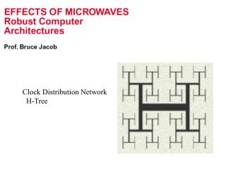
2. Clock Distribution Network • H-tree as clock dist. Network • clock receiver(photo-diode) at the center receiving sharp laser pulse through a glass window in the package
Composition of a PLL(Phase-Locked Loop) i) Loop filter : • loop filter is introduced to remove clock jitter. • 1st to 3rd-order LPF is generally needed, as excessive phase shift due to high-order filtering can cause instability in this feedback structure. ii) Lock range : range of input frequency over which output follows input frequency over which output follows input with given relationship. iii) Lock time : time for PLL to lock into the input iv) Jitter : Loop filter(LPF) helps remove jitter.
Simply generating local clocks from global clock generates clock skew causing inter-chip communication impossible.
Global Clock Source • How to minimize clock skew in multi-chip system, i.e., board or multiple-board system. i) Global dist. Network. ii) On-chip clock generator/buffer PLL can help here only. iii) Local dist. Network.
Each Component of Skew : i) Chip-to-chip clock skew due to global dist. Network ; can be suppressed by ; • placing clock pins/pads at the identical positions on the chip carrier/chip. • Keeping the lead length and capacitive loading of clock pins and wires from the global clock source to each clock pin as identical as possible. ii) Skew due to on-chip clock generator/buffer can be suppressed by PLL;
Each Component of PLL(Phase detector, LPF, voltage-controlled delay line)
Methodology for dealing with timing problems in LARGE systems ; 1) Divide the whole system into a number of regions, with each region operating in synchronous manner. 2) Communication among each region is either i) through a global clock slower(N) than local clock or ii) asynchronously using self-timed discipline.
Using PLL for local synchronization between global & local clocks. Delay of local clock is adjusted via. PLL to make the local clock edge occurring simultaneously with global clock edge.
Minimal skew system 1) equal-length chip-to-chip interconnection 2) PLL-based clock generator/buffer, and 3) equal-length on-chip distribution(H-tree)
Symmetric clock trees(H- vs X- tree) - H-tree is better than X-tree in that i) in H-tree, no corners sharper than 90, thus with smaller inductive discontinuity, reflection is small. ii) in H-tree, fan-out is only 2, simplifying impedance matching
Reduction of inductive discontinuities at the corners of H-tree.
Zk+1 2 Zk+1 • Matching condition at the branch point : - impedance matching occurs when Zk=Zk+1//Zk+1= Zk Zk+1
Sharpening clock signal at the receiver front before distribution in the subblock using schmitt trigger or source-end-terminated buffer.(Look at sharp rise of Vb in previous slide.)
RC network representation of H-clock tree(simplified as a distributed RC line): When tailored H-clock tree is used, I.e., if the line width is halved at each branching point, above distributed RC tree network is equivalent to a uniformly distributed RC line.(R1= R2= R3=…, C1=2C2=4C3=...)
Requirement of the cross-sectional geometry(height, width) of interconnection line : 1) From distributed RC model ; • Total distance from clock source to end point(ltot) in H-tree : • Time required for the last node to reach 90% of its final value : Rint : resistance of interconnection per unit length Cint : capacitance per unit length
2) From lossy transmission line RC model : Eq. (1), (2) need to be considered in determining H&W. For high frequency, skin effect prevents thickening the interconnection by more than 2-4 times the skin depth ineffective. For 1GHz, skin depth of aluminum is 2.8m.
3. Self-Timed Logic Circuits • Synchronous vs. Asynchronous(Self-Timed) i) In pipelined systems, performance(throughput) depends on worst case stage delay in synchronous systems, while it depends on average delay in self-timed systems. ii) (cons of synchronous system) : Distribution of high-speed clock over all region is a very difficult problem. iii) (cons of asynchronous systems) : Hand-shaking logic overhead.
Pipelined, synchronous datapath : • Self-timed pipelined datapath : R1 F1 R2 F2 R3 F3 R4 In Out tpF1 tpF2 tpF3 tpreg 5 1 Req Req Req Req HS HS HS 2 6 Ack Ack Ack Ack 3 4 7 Start Done 8 Start Done Start Done R1 F1 R2 F2 R3 F3 In Out tpF1 tpF2 tpF3
Sequence of Events : i) As input word arrives at the input of R1, I.e., at the input buffer(IN buffer) Req(to F1) is raised. If F1 is then available(inactive), data is transferred to R1 and Acknowledges it to IN buffer. ii) F1 is then enabled by ‘start’ signal ‘Done’ signal goes high indicating the completion of the computation. iii) Request to F2-module is issued. If F2 is available, Ack is raised, and the output from F1 is transferred to R2. F1 continues with its next sample for computing.
Completion(Done) signal generation : - redundant signal generation. Ex. 2bit per signal : 00 : out 0 11 : out 1 01 or 10 : out retains its current value. B B0 B1 in transition(or reset) 0 0 0 0 1 1 1 0 illegal 1 1
An example showing Muller C-element. 1) 2) 2-, self-timed FIFO
4-cycle(4-phase) handshaking protocol : ex) Implementation of 4-phase handshaking protocol
Muller C element : • Its output is 1 when all inputs are 1, and 0 when all inputs are 0 ; otherwise remains at its earlier state. • Called as rendezvous, join or last-of circuit.
Conversion between single rail plus request and double rail data : single single double