Download
1 / 37
370 likes | 425 Views
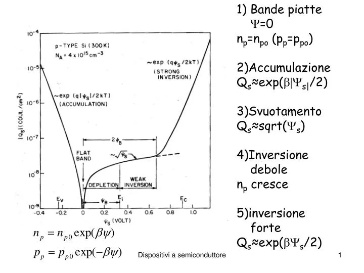
Bande piatte =0 n p =n po (p p =p po ) 2)Accumulazione Q s ≈exp( s| /2) 3)Svuotamento Q s ≈sqrt( s ) 4)Inversione debole n p cresce 5)inversione forte Q s ≈exp( s /2). Applicazioni.

E N D
Bande piatte =0 np=npo (pp=ppo) 2)Accumulazione Qs≈exp(s|/2) 3)Svuotamento Qs≈sqrt(s) 4)Inversione debole np cresce 5)inversione forte Qs≈exp(s/2) Dispositivi a semiconduttore
Applicazioni “Tuning” del numero e tipo portatori vicino alla superficie del semiconduttore ( appl. CCD -1969 Boyle-Smith ) Dispositivi a semiconduttore
2 1 3 Regime di deep depletion Con sequenza clock si ha immagazzinamento e trasferimento carica Dispositivi a semiconduttore
Transistor bipolare Transfer resistor:dispositivo a 3 terminali in cui la resistenza fra 2 terminali è controllata dal terzo terminale E’ un dispositivo bipolare perchè la corrente è trasportata da due tipi di portatori Bell Labs 1947: Bardeen & Brittain point contact transistor 1949: Teoria di Shockley per giunzioni p-n 1951:I dimostrazione di un transistor bipolare 1956: Nobel a Bardeen & Brittain e Shockley Dispositivi a semiconduttore
An amazingly simple device, capable of performing efficiently nearly all the functions of an ordinary vacuum tube, was demonstrated for the first time yesterday at Bell Telephone Laboratories where it was invented. Known as the Transistor, the device works on an entirely new physical principle discovered by the Laboratories in the course of fundamental research into the electrical propertiesof solids. Although the device is still in the laboratory stage, Bell scientists and engineers expect it may have far-reaching significance in electronics and electrical communication. The whole apparatus is housed in a tiny cylinder less than an inch long. It will serve as an amplifier or an oscillator -- yet it bears almost no resemblance to the vacuum tube now used to do these basic jobs. It has no vacuum, no glass envelope, no grid, no plate, no cathode and therefore no warm-up delay. Two hair-thin wires touching a pinhead of a solid semi- conductive material soldered to a metal base, are the principal parts of the Transistor. These are enclosed in a simple, metal cylinder not much larger than a shoe-lace tip. More than a hundred of them can easily be held in the palm of the hand. Since the device is still in the experimental stage, no data on cost are available. Its essential simplicity, however, indicates the possibility of widespread use, with resultant mass- production economies. When fully developed, the Transistor is also expected to find new applications in electronics where vacuum tubes have not proved suitable. Tests have shown that the Transistor will amplify at least I00 times (20 decibels). Some test models have been operated as amplifiers at frequencies up to ten million cycles per second. Because of the basically simple structure of the new units, stability and long life are expected. Dispositivi a semiconduttore
La definizione di lacuna…. Transistoractiondependsuponthefactthatelectrons inasemi-conductorcancarrycurrentintwodistinctlydifferent ways.Thisisbecausemostoftheelectronsinasemiconductor donotcontributetocarryingthecurrentatall.Insteadthey areheldinfixedpositionsandactasarigidcementtobind togethertheatomsinasolid.Onlyifoneoftheseelectrons getsoutofplace,orifanotherelectronisintroducedinone ofanumberofways,cancurrentbecarried.If,ontheother hand,oneoftheelectronsnormallypresentinthecementis removed,thenthe"hole"leftbehinditcanmovelikeabubble inaliquidandthuscarrycurrent. Dispositivi a semiconduttore
Giunzione np Dispositivi a semiconduttore
p n Giunzione np p n Dispositivi a semiconduttore
Corrente giunzione pn Dispositivi a semiconduttore
Due giunzioni separate con polarizzazione opposta Reverse p n n Forward Dispositivi a semiconduttore
p n n Due giunzioni vicine Dispositivi a semiconduttore
Nobel 1956 Dispositivi a semiconduttore
PNP NPN Transistor In genere la regione di emettitore ha drogaggio più alto rispetto al collettore Dispositivi a semiconduttore
VEB VBC p n p Emettitore Base Collettore r -xE xC W x Dispositivi a semiconduttore
VEB VBC p n p Emettitore Base Collettore r -xE xC W x Dispositivi a semiconduttore
Transistor Dispositivi a semiconduttore
5 e 6 sono correnti trascurabili Dispositivi a semiconduttore
N-P-N Dispositivi a semiconduttore
N-P-N Dispositivi a semiconduttore
Componenti corrente N-P-N Giunzione E-B: corrente di diffusione di elettroni e lacune Nella base: Ricombinazione e se base sottile transito elettroni Nel collettore: raccolta elettroni InE: corrente diffusione elettroni InC: corrente diffusione elettroni raccolti al collettore IrB= InE-InC: ricombinazione in base IpE: corrente di diffusione lacune E-B IrE: ricombinazione E-B ICO: corrente inversa C-B Dispositivi a semiconduttore
Lacune nella base Dispositivi a semiconduttore
Distribuzione portatori minoritari Dispositivi a semiconduttore
Parametri Efficienza di emettitore Dispositivi a semiconduttore
Fattore di trasporto nella base Guadagno a base comune Dispositivi a semiconduttore
Parametri Dispositivi a semiconduttore
Parametri Dispositivi a semiconduttore
Parametri Dispositivi a semiconduttore