Download
1 / 16
160 likes | 181 Views
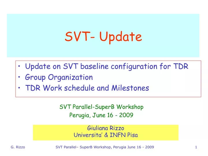
SVT- Update. Update on SVT baseline configuration for TDR Group Organization TDR Work schedule and Milestones. SVT Parallel-SuperB Workshop Perugia, June 16 - 2009. Giuliana Rizzo Universita’ & INFN Pisa. Hybrid Pixels. CMOS DNW MAPS. Wafer bonding & electrical interconn.

E N D
SVT- Update Update on SVT baseline configuration for TDR Group Organization TDR Work schedule and Milestones SVT Parallel-SuperB Workshop Perugia, June 16 - 2009 Giuliana Rizzo Universita’ & INFN Pisa SVT Parallel– SuperB Workshop, Perugia June 16 - 2009
Hybrid Pixels CMOS DNW MAPS Wafer bonding & electrical interconn. Digital tier Analog tier Sensor Pixels with Vertical Integration SVT Update R&D work reorganized to prepare a baseline for TDR with: • Layer0 based on hybrid pixels: • Better chance (w.r.t to newer technologies) to meet the Layer0 requirements for the TDR timescale • 50x50 mm2 pitch - first front-end chip & pixel sensor in production in Sept. ‘09. • R&D on pixel module support/cooling & interfaces (similar for all pixel options) • Layer1-Layer5 similar to BaBar SVT Layer0 pixel options under study Talks in the SVT parallels Lower material & improved performance Continue R&D on thin pixels technology (SLIM5VIPIX Collaboration-INFN) • CMOS DNW MAPS + Vertical Integration technology very promising for Layer 0 but not yet mature for TDR timescale. • First DNW MAPS chip realized with two thin CMOS layers interconnected first results by end of 2009 if positive could be seriously considered for Layer0 performance improvement SVT Parallel– SuperB Workshop, Perugia June 16 - 2009
Agenda of the SVT Parallels • Tuesday 16 June 16-17:30 • Introduction – Rizzo • SVT Backgrounds - Present knowledge E. Paoloni • Front-end analog cell optimization for hybrid pixel sensors – G. Traversi • First results on Apsel5T Bettarini • Wednesday 17 June 9-10:30 • Radiation Damage Studies on DNW MAPS – L. Ratti • Vertical Integration Activities – V. Re • Pixel Readout Architecture Optimization - Simulation Results - F. Giorgi • Wednesday 17 June 11-12:30 • Pixel Module Interfaces – M. Citterio • SVT Mechanics – F. Bosi • Layer0 support & cooling M. Massa • Discussion SVT Parallel– SuperB Workshop, Perugia June 16 - 2009
Layer0 20 cm 30 cm 40 cm SVT baseline configuration LayerRadius 0 1.5 cm 1 3.3 cm 2 4.0 cm 3 5.9 cm 4 9.1 to 12.7 cm 5 11.4 to 14.6 cm Layer 0: Hybrid Pixels Radius~1.5 cm, Module length~10 cm Power consumption ~ 2 W/cm2 in the active area Total material budget ~ 1% X0 • Si sensor + FE chips 0.40 % X0 • Al Bus + SMD comp. 0.34 % X0 • Support & cooling ~ 0.3% X0 SuperB Interaction Region Schematic SVT superimposed • CF Support with microchannels technology is within specs with material ~ 0.3% X0 External Layers: Baseline similar to the present BaBar SVT: double sided silicon detectors 300 um thick • Assume same BaBar radii for the 5 layers • L1-L2-L3 barrel shape • L4-L5 arch shape • Extend coverage down to 300 mrad FW and BW • In BaBar it was 300 mrad FW and 520 mrad BW SVT Parallel– SuperB Workshop, Perugia June 16 - 2009
SVT SW related studies • Background Studies – News in the next talk by E. Paoloni • Implementation of the SVT baseline in FastSim and first performance results will be presented in other parallel session: • Wednesday 17 June 2009 • 14:00->15:30 Parallel - Tracking (DGWG) • Tracking Performance with the SVT baseline configuration - N. Neri • Boost sensitivity on time dependent measurements - N. Neri • 16:00->17:30 Parallel - Fast Simulation • Resolution model for pixels with digital readout - J. Walsh • SVT passive material implementation in FastSim - M. Bomben SVT Parallel– SuperB Workshop, Perugia June 16 - 2009
SVT Group Organization & Update • Regular SVT bi-weekly meeting for TDR started in April. (Tue– 17:15 CET) • WBS and TDR work schedule prepared. Preliminary outcome in the next slides. SVT – management structure (responsibility for TDR preparation) SVT Parallel– SuperB Workshop, Perugia June 16 - 2009
Summary of the SVT - WBS • Small changes still under way • Missing Manpower • Eng Mech: • 1 FTE Layer0 & beam pipe • ~1 FTE external layers and support structure • Eng. Electr: • 1 FTE layer0 technology • 0.5 FTE electrical system eng.+det monitoring & interlock • Physicist: • 1 FTE missing on SVT-DAQ • 0.5 FTE background simulation Request for SVT contracts (Regione Lazio funding) 1 FTE Mechanical Eng. – Pisa - • Design Layer0, beam-pipe and IR. Simulation with FEM Layer0, beam-pipe cooling systems. 1 FTE Electronic Eng. - Pavia • Design analog and digital blocks for processing of signals silicon pixel in ultra-deep submicron CMOS technology. Power distribution in FE pixel chips, radiation damage, test fabricated chips 1 FTE Physicist - Bologna • DAQ development for lab and beam tests; SVT DAQ architecture/optimization studies; Electronic board integration into a global DAQ framework; SVT trigger studies. 1 FTE Physicist (sharing with computing) – Milano • GDML coding for the SVT geometry. Machine backgrounds studies for SVT. • Implement SVT front end electronic response in the Geant4 simulation framework. SVT Parallel– SuperB Workshop, Perugia June 16 - 2009
TDR work schedule & Milestones (I) Preliminary Hybrid Pixels (baseline for TDR) • High resistivity Pixel sensor batch submission Sept 2009 • Optimization of the front-end readout architecture on full size matrix – May ’09 (internal) • Optimization of the analog cell design – June‘09 (internal) • Small front-end prototype chip submitted with ST technology Sept 2009 MAPS (Possible option for performance improvement:inTDR report on R&D progress) • Radiation Damage results 12/2009 (internal) • Power distribution on large matrix 12/2009 (internal) • MAPS Apsel5d (40 mm2) choice of technology (ST vs Chartered/Tezzaron) 11/2009 • Apsel5D in production Jan-2010 (if ST) or ~March 2010 (if Chartered/Tezzaron) Pixel module interfaces • Completion of the "construction" of a first prototype (simplified version) of the Layer 0 multi-layer aluminum-based BUS - Sept. 2009 • Definition of HDI and link specification (chip-to-HDI and HDI-to-DAQ) - Oct. 2009 • Choice of technology for the HDI integrated circuits (memory, buffers, drivers) - Dic. 2009 (internal) • Submission of a test chip (simple and complex circuits blocks) based on the chosen technology - Mar. 2010 • Tests on the full link (by means of FPGAs+Al-BUS+copper/fiber link) - Apr. 2010 External Layers • Module components specs definition (sensor, fanout, front-end chip) Oct/2009 • Evaluate different front-end chips SVT Parallel– SuperB Workshop, Perugia June 16 - 2009
TDR work schedule & Milestones (II) Preliminary Testbeam • Testbeam 9/2010 with large MAPS matrix + Hybrid pixel sensor+FE chip prototype (internal until schedule on next items is not clear) • If large MAPS matrix is submitted in March (Chartered technology chosen) and bump bonding of hybrid pixel sensor+FE chip is not ready by June 2010 the testbeam should be postponed at the end of 2010 (too late for TDR?) DAQ • Complete design for testbeam DAQ board 12/2009 • DAQ system for TDR still has too many unknowns (data push vs triggered, link module-DAQ board) Mechanics • First thermal and mechanical characterization of Layer0 module support for hybrid pixel, realized with CF microchannels and the additive method: June 2009 • Hydraulic flanges prototype for layer0 modules & conclude R&D on Layer0 module support: from June to Oct 2009 • Full layer0 support design: June 2009-Sept 2010 • Solid modeling of IR based on present design: first iteration by June – 2009 • Recover all design from BaBar SVT by June 2009 • First design of the mechanical support , based on BaBar SVT (modules, space frame, support cones or other similar solutions) with the new SuperB IR: Dec 2009(?) • Possible alternative Mechanical Support design to allow fast L0/SVT dismounting: Oct 2009-Sept.2010 • Beam Pipe design: June 2009-Sept2010 SVT Parallel– SuperB Workshop, Perugia June 16 - 2009
TDR work schedule & Milestones (III) Preliminary Detector Optimization Studies(Still need to work on a the schedule after June 2009) • Implement Baseline SVT configuration in Fastsim (realistic version): June 2009 • Material, resolution model for 50 um pitch, extend external layers to 300 mrad, realistic passive material in active area. • dE/dx and realistic modeling of the material at the edge of the coverage might require more time. • Test layer 0 performance for time dependent analysis (channel phi Ks) with realistic baseline: June 2009 • Extend geometry to 200 mrad to allow study in DGWG (Help from DGWG people) • Evaluate performance (tracking and time dependent analysisi) with L0+L1 made of hybrid pixel .by Oct 2009? • External Layer optimization (channel Ks pi0) : efficiency, resolution, evaluate error on asymmetry with toy MC: by Oct-Dec 2009? SVT Parallel– SuperB Workshop, Perugia June 16 - 2009
Goals of this wokshop • Review progress in development areas • Define the TDR work timeline • Review schedule shown in the previous slides during the discussion at the end of the SVT parallel session on Wed morning. • From FastSim results: performance evaluation with different tracker configurations (SVT-DCH transition, SVT radii) • Help to define SVT baseline for external layers configuration • For Layer0 we will do our best in term of sustainable radial position (background!) & material • Integration SVT/Interaction Region • Starting point to design SVT support structure with easy access/replacement for Layer0/IR beam pipe. SVT Parallel– SuperB Workshop, Perugia June 16 - 2009
backup SVT Parallel– SuperB Workshop, Perugia June 16 - 2009
Layer 0 pixel R&D activities 1. Hybrid Pixels: - Sept 2009 produce small prototype Front-End chip for hybrid pixel: • 50x50 um pitch, 32x 128 pixel matrix, STMicroelectronics 130 nm • same readout architecture data push developed for MAPS with optimization: • Simulation for full size matrix (256x180 pixels) should have readout efficiency ~ 98% with 100 MHz/cm2 hit rate • reoptimize analog cell (small capacitance ~ 50-100 fF, high signal from MIP with fully depleted 200 um substrate) • significant reduction in the analog power consumption w.r.t MAPS chip ~ 1 uA/pixel (?) • Power consumption for digital section dominates ~ 1W/cm2 - Sept 2009 produce pixel sensors (ITC, IRST) - Test with beam Sept 2010: pixel sensor bump bonded to the FE chip. • Bump bonding could be an issue since we will not have the full wafer for the FE chips. 2. Develop Pixel module components, hybrid pixel & MAPS (next slide) 3. Continue R&D on MAPS: - Large Matrix (APSEL5D~40 mm2 active area) in production beginning of 2010 - Radiation damage studies (Co60 up to 5 Mrad, Neutron irradiation to start) - Testbeam on APSEL5D in Sept. 2010, single chip (no time for MAPS mod. integration). - Later testbeam (post TDR with MAPS module) At the time of the TDR report on progress on MAPS, possible option for performance improvements. Design Layer0 easily accessible for replacement SVT Parallel– SuperB Workshop, Perugia June 16 - 2009
Pixel module for Layer 0 • Plan proposed in CSN1 in Sept. 2008: build a multichip CMOS MAPS prototype module with specs close to the SuperB Layer0 requirements. • Activity started document with specs for MAPS module components. Module components very similar for Layer0 based on Hybrid Pixels. Produce a new document with specs for Hybrid Pixels components SVT Parallel– SuperB Workshop, Perugia June 16 - 2009
Pixel module for Layer 0 Pixel module components • Pixel BUS needs: low material, many lines, high frequency (> 100 MHz), • contact started with CERN PCB shop (produce and test Al prototypes) • Different options under study on Interfaces (HDI- power/signal input and data output link) & SVT data transmission • Layer 0 module rates: 20 Gbit/s full rate (FE data push), 3 Gbit/s triggered rate • Use modified EDRO board (SLIM5) with large FPGA, memory and optical links (i.e. flexible)as interface between FE chips and SuperB trigger and DAQ. SVT Parallel– SuperB Workshop, Perugia June 16 - 2009
SVT configurations in FastSim • SVT baseline configuration (as in slide 7: Layer0 hybrid pixel + Layer1-Layer5 similar to BaBar SVT) will be used by the Detector Geometry Working Group for Physics Studied. • N.Neri is working to update the SVT baseline description in FastSim (realistic evaluation of material, resolution etc) • Other configurations will be evaluated using the FastSim for the optmization of the SVT internal geometry • Layer0 and Layer1 with hybrid pixels + BaBar SVT configuration for Layer2 – Layer 5 • This could become a serious option if the background at Layer 1 location is much higher than what is quoted in the CDR. • Layer0 hybrid pixels with pitch 50x250 μm2 (z, r-phi) as foreseen for Atlas B-Layer upgrade. Well advanced project with specs and timescale similar to SuperB • Optimization of the external layers position and shape (number of layers; radius of each layer; arch-shape, barrel-shape or disks) SVT Parallel– SuperB Workshop, Perugia June 16 - 2009