Download
1 / 51
510 likes | 531 Views
The RX210 Group features the MTU2, a 16-bit timer with multiple operations including PWM modes, synchronous operation, and interrupt sources. Learn about basic timer functions, counter operation, and compare match actions. Discover how the MTU2 facilitates diverse timing applications on a microcontroller platform.

E N D
Outline • Basic Operation • Synchronous Operation • PWM Modes • Interrupt Sources • Registers
Timer • Timer is a counter which counts clock pulses of the microcontroller clock • The value in timer register increases with each clock cycle and overflows to zero after reaching to its maximum count • The time can be measured as : • Time= timer register/clock frequency • For example, 8-bit timer with 10MHz clock frequency can measure maximum of : • (2^8) / 10MHz = 25.5us
Prescaler • In the last example, the timer could measure only 25.5us before resetting • Prescaler setting can be used to increase this measured time • Suppose prescaler is set to 64, the timer register will increment by 1 after 64 clock cycles • So the same timer can measure a maximum time of : [(2^8) / 10MHz ] * 64 = 1.63 ms
Overview The RX210 Group has a on-chip multi-function timer pulse unit 2 (MTU) Each unit comprises a 16-bit timer with six channels MTU0 to MTU5 Available operations Waveform output at compare match Input capture function (noise filter set function) Counter clear operation Simultaneous writing to multiple timer counters (TCNT) Simultaneous clearing by compare match or input capture Simultaneous register I/O by synchronous counter operation A maximum of 12-phase PWM output is available in combination with synchronous operation 8 clocks or 7 clocks for each channel (4 clocks for MTU5) A/D converter start trigger can be generated
Basic Operation Each channel has TCNT and TGR TCNT performs up-counting Also capable of free-running operation, periodic counting, and external event counting Each TGR can be used as an input capture register or an output compare register Counter Operation TCNT for the corresponding channel begins counting When one of bits CST0 to CST4 in TSTR or bits CSTU5, CSTV5, and CSTW5 in MTU5.TSTR is set to 1 Free-Running Count Operation Immediately after a reset, the MTU’s TCNT counters are all designated as free-running counters When the relevant bit in TSTR is set to 1, the TCNT counter starts up-count operation as a free-running counter When TCNT overflows (from FFFFh to 0000h), the MTU requests an interrupt if the corresponding TCIEV bit in TIER is 1
Basic Operation (cont.) After an overflow, TCNT starts counting up again from 0000h Periodic Count Operation TCNT for the relevant channel performs periodic count operation When compare match is selected as the TCNT clearing source TGR is designated as an output compare register for setting the cycle Counter clearing by compare match is selected by means of bits CCLR[2:0] in TCR After the settings have been made, TCNT starts up-count operation when the corresponding bit in TSTR is set to 1 When the count matches the value in TGR, TCNT is cleared to 0000h If the value of the corresponding TGIE bit in TIER is 1 at this point, the MTU requests an interrupt After a compare match, TCNT starts counting up again from 0000h
Basic Operation (cont.) Free-Running Count Operation Periodic Count Operation
CompareMatch • We can take an action like toggling an output signal or triggering an interrupt when the timer count reaches a preset value • A match occurs when count register value TCNT reaches the preset compare match register TGR
Basic Operation (cont.) Waveform Output by Compare Match The MTU can output low or high or toggle output from the corresponding output pin using compare match
Basic Operation (cont.) An example of low output and high output TCNT has been designated as a free-running counter Settings: High is output by compare match A Low is output by compare match B When the pin level is the same as the specified level, the pin level does not change
Basic Operation (cont.) An example of toggle output TCNT has been designated as a periodic counter With counter clearing on compare match B Settings: The output is toggled by both compare match A and compare match B
Basic Operation (cont.) Input Capture Function The TCNT value can be transferred to TGR on detection of the MTIOC pin input edge The rising edge, falling edge, or both edges can be selected as the detection edge For MTU0 and MTU1, another channel’s counter input clock or compare match signal can be specified as the capture source
Basic Operation (cont.) An example of input capture operation Both rising and falling edges have been selected as the MTIOCnA pin input capture input edge The falling edge has been selected as the MTIOCnB pin input capture input edge Counter clearing by TGRB input capture has been made
Synchronous Operation The values in multiple TCNT counters can be modified simultaneously (synchronous presetting) Multiple TCNT counters can be cleared simultaneously (synchronous clearing) by making the proper setting in TCR Synchronous operation increases the number of TGR registers assigned to a single time base MTU0 to MTU4 can all be designated for synchronous operation MTU5 cannot be used for synchronous operation An example of synchronous operation Synchronous operation and PWM mode 1 have been designated for MTU0 to MTU2 MTU0.TGRB compare match has been set as the counter clearing source in MTU0 Synchronous clearing has been set for the counter clearing source in MTU1 and MTU2 Three-phase PWM waveforms are output from pins MTIOC0A, MTIOC1A, and MTIOC2A
Synchronous Operation (cont.) Synchronous presetting and synchronous clearing by MTU0.TGRB compare match are performed for the TCNT counters in MTU0 to MTU2 The data set in MTU0.TGRB is used as the PWM cycle
Buffer Operation Provided for MTU0, MTU3, and MTU4 Enables TGRC and TGRD to be used as buffer registers In MTU0, TGRF can also be used as a buffer register Buffer operation differs depending on Whether TGR has been designated as an input capture register or as a compare match register The register combinations used in buffer operation
Buffer Operation (cont.) When TGR is an output compare register When a compare match occurs The value in the buffer register for the corresponding channel is transferred to the timer general register When TGR is an input capture register When an input capture occurs The value in TCNT is transferred to TGR and the value previously held in TGR is transferred to the buffer register
Buffer Operation (cont.) Buffer Operation Setting Procedure An operation example of the output compare register PWM mode 1 has been designated for MTU0 Buffer operation has been designated for TGRA and TGRC TCNT clearing by compare match B High output at compare match A The TTSA bit in MTU0.TBTM is set to 1 When compare match A occurs, the output changes
Buffer Operation (cont.) The value in buffer register TGRC is simultaneously transferred to timer general register TGRA This operation is repeated each time compare match A occurs An operation example of the input capture register TGRA has been designated as an input capture register Buffer operation has been designated for TGRA and TGRC
Buffer Operation (cont.) Counter clearing by TGRA input capture has been set for TCNT Both rising and falling edges have been selected as the MTIOCnA pin input capture input edge When the TCNT value is stored in TGRA upon occurrence of input capture A, the value previously stored in TGRA is simultaneously transferred to TGRC
Buffer Operation (cont.) The timing for transfer from buffer registers to TGR registers Either compare match (initial setting) or TCNT clearing can be selected for the transfer timing Can be selected in PWM mode 1 or 2 for MTU0 Or in PWM mode 1 for MTU3 and MTU4 By setting the buffer operation transfer mode registers (MTU0.TBTM, MTU3.TBTM, and MTU4.TBTM) TBTM must be modified only while TCNT stops TCNT clearing as transfer timing is one of the following cases: When TCNT overflows (FFFFh → 0000h) When 0000h is written to TCNT during counting When TCNT is cleared to 0000h under the condition specified in the CCLR[2:0] bits in TCR An operation example PWM mode 1 is designated for MTU0 Buffer operation is designated for MTU0.TGRA and MTU0.TGRC
Buffer Operation (cont.) MTU0.TCNT clearing by compare match B High output at compare match A Low output at compare match B The TTSA bit in MTU0.TBTM is set to 1
PWM Modes Provided to output PWM waveforms from the external pins The output level can be selected as low, high, or toggle output in response to a compare match of each TGR PWM waveforms in the range of 0% to 100% duty cycle can be output according to the TGR settings By designating TGR compare match as the counter clearing source, the PWM cycle can be specified in that register Every channel can be set to PWM mode independently Synchronous operation is also possible PWM Mode 1 PWM waveforms are output from the MTIOCnA and MTIOCnC pins by pairing TGRA with TGRB and TGRC with TGRD The levels specified by bits IOA3 to IOA0 and IOC3 to IOC0 in TIOR are output from the MTIOCnA and MTIOCnC pins at compare matches A and C The levels specified by bits IOB3 to IOB0 and IOD3 to IOD0 in TIOR are output at compare matches B and D
PWM Modes (cont.) The initial output value is set in TGRA or TGRC If the values set in paired TGRs are identical, the output value does not change even when a compare match occurs PWM Mode 2 PWM output is generated using one TGR as the cycle register and the others as duty registers The level specified in TIOR is output at compare matches Upon counter clearing by a synchronized register compare match, the initial value set in TIOR is output from each pin If the values set in the cycle and duty registers are identical, the output value does not change even when a compare match occurs In PWM mode 2, up to eight phases of PWM waveforms can be output when using synchronous operation in combination The correspondence between PWM output pins and registers is listed:
PWM Modes (cont.) The PWM mode setting procedure
PWM Modes (cont.) An example of operation in PWM mode 1 TGRA compare match is set as the TCNT clearing source Low is set as the initial output value and output value for TGRA High is set as the output value for TGRB The value set in TGRA is used as the cycle The value set in TGRB is used as the duty An example of operation in PWM mode 2 Synchronous operation is designated for MTU0 and MTU1 MTU1.TGRB compare match is set as the TCNT clearing source
PWM Modes (cont.) Low is set as the initial output and output values for TGRB High as the output value for the other TGR registers (MTU0.TGRA to MTU0.TGRD and MTU1.TGRA) Outputting 5-phase PWM waveforms The value set in MTU1.TGRB is used as the cycle The values set in the other TGRs are used as the duty
Phase Counting Mode The phase difference between two external input clocks is detected TCNT is incremented or decremented accordingly This mode can be set for MTU1 and MTU2 When this mode is specified, an external clock is selected as the counter input clock TCNT operates as an up/down-counter regardless of the setting of bits TPSC[2:0] and bits CKEG[1:0] in TCR The functions of bits CCLR[1:0] in TCR and of TIOR, TIER, and TGR are valid Input capture/compare match and interrupt functions can be used If an overflow occurs, a TCIV interrupt is generated While the TCIEV bit in the corresponding TIER is 1 If an underflow occurs, a TCIU interrupt is generated While the TCIEU bit in the corresponding TIER is 1
Phase Counting Mode (cont.) The TCFD bit in TSR is the count direction flag Read the TCFD flag to check whether TCNT is counting up or down The phase counting mode setting procedure.
Phase Counting Mode (cont.) Phase counting mode 1
Phase Counting Mode (cont.) Phase counting mode 2
Phase Counting Mode (cont.) Phase counting mode 3
Phase Counting Mode (cont.) Phase counting mode 4
Interrupt Sources There are three kinds of MTU interrupt source TGR input capture/compare match, TCNT overflow, and TCNT underflow Each interrupt source has its own enable/disable bit Allowing the generation of interrupt request signals to be enabled or disabled individually When an interrupt source is detected, an interrupt is requested If the corresponding enable/disable bit in TIER is set to 1 Relative channel priorities can be changed by the interrupt controller The priority within a channel is fixed Input capture/compare match interrupt If the TGIE bit in TIER is set to 1 When a TGR input capture/compare match occurs on a channel The MTU has 21 input capture/compare match interrupts Six for MTU0, four each for MTU3 and MTU4, two each for MTU1 and MTU2, and three for MTU5
Interrupt Sources (cont.) Overflow interrupt If the TCIEV bit in TIER is set to 1 When a TCNT overflow occurs on a channel The MTU has five overflow interrupts One for each channel Underflow interrupt If the TCIEU bit in TIER is set to 1 When a TCNT underflow occurs on a channel The MTU has two underflow interrupts One each for MTU1 and MTU2 (Phase Counting) The DTC can be activated by the TGR input capture/compare match interrupt in each channel or the overflow interrupt in MTU4 The DMAC can be activated by the TGRA input capture/compare match interrupt in each channel
Interrupt Sources (cont.) The A/D converter can be activated The A/D converter can be activated by the occurrence of a TGRA input capture/compare match in each channel A compare match between MTU0.TCNT and MTU0.TGRE activates the A/D converter A compare match between MTU0.TCNT and MTU0.TGRF activates the A/D converter The A/D converter can be activated when an input capture or compare match occurs between MTU0.TCNT and MTU0.TGRB The A/D converter can be activated by generating A/D converter start request signal TRG4AN or TRG4BN When the MTU4.TCNT count matches the TADCORA or TADCORB value if the UT4AE, DT4AE, UT4BE, or DT4BE bit in the A/D converter start request control register (TADCR) is set to 1
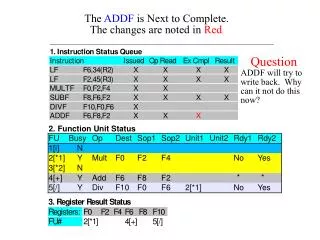
Registers Timer Counter (TCNT) The MTU has a total of eight TCNT counters One each for MTU0 to MTU4 Three (MTU5.TCNTU, TCNTV, and TCNTW) for MTU5 A 16-bit readable/writable counter Timer General Register (TGR) The MTU has a total of 21 TGR registers Six for MTU0, two each for MTU1 and MTU2 Four each for MTU3 and MTU4, and three for MTU5 TGR is a 16-bit readable/writable register Can also be designated for operation as buffer registers
Registers (cont.) Timer Start Registers (TSTR) TSTR (MTU0 to MTU4) and TSTR (MTU5)
Registers (cont.) Timer Interrupt Enable Register (TIER)
Registers (cont.) Timer Control Register (TCR)
Registers (cont.) Timer Status Register (TSR)
Registers (cont.) Timer I/O Control Register (TIOR)
Registers (cont.) Timer Synchronous Registers (TSYR)
Registers (cont.) Timer Mode Register (TMDR)