Download
1 / 6
60 likes | 163 Views
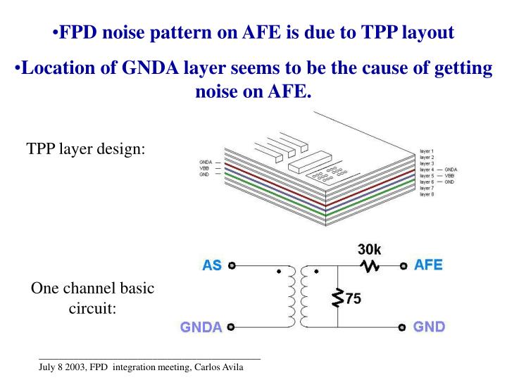
FPD noise pattern on AFE is due to TPP layout Location of GNDA layer seems to be the cause of getting noise on AFE. TPP layer design:. One channel basic circuit:. Tests on AFE phase 5 stand. Primary ground out. Used an empty TPP board and added transformers to only one ribbon connector.

E N D
FPD noise pattern on AFE is due to TPP layout • Location of GNDA layer seems to be the cause of getting noise on AFE. TPP layer design: One channel basic circuit:
Tests on AFE phase 5 stand Primary ground out • Used an empty TPP board and added transformers to only one ribbon connector. • Took out the primary ground of transformers. • extended one ribbon cable from pw08 to phase 5 test stand • Tested different ground configurations
PW08 cable connected to MCM4 on phase 5 stand 9.0 MCM4 2.5 MCM4 3.5 MCM4
RMS on MCM2 with pw08 cable connected on MCM4 10.0 MCM2 1.6 MCM2 3.0 MCM2
Another Possibility is not connecting primary ground to any layer, just connect primary ground to the ground on input ribbon cable. 4.0 MCM4 MCM4 July 6 July 3 2.0 MCM2
SUMMARY AND CONCLUSIONS • Two possible TPP configurations to reduce noise: • Not connecting primary ground to a layer plane reduces noise pickup on different lines. • Waiting for Collision Hall access to perform tests at Pw08 • If we want new boards made, it would take about one week to get new Gerber file if we just swap VBB and GNDA layers. It would take about a month to make major modifications + time of making the boards + time to stuff them. We could also just rewire the board: