Download
1 / 37
370 likes | 494 Views
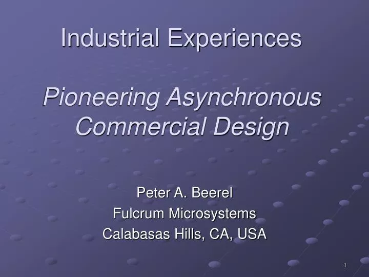
Industrial Experiences Pioneering Asynchronous Commercial Design. Peter A. Beerel Fulcrum Microsystems Calabasas Hills, CA, USA. Specification. Design & Verification. Design & Verification. Simulation & Verification. Synthesis & Floor Planning. Physical Design.

E N D
Industrial ExperiencesPioneering Asynchronous Commercial Design Peter A. Beerel Fulcrum Microsystems Calabasas Hills, CA, USA
Specification Design & Verification Design & Verification Simulation & Verification Synthesis & Floor Planning Physical Design Database Release to Manufacturing Agenda • Introduction to Fulcrum • Description of Integrated Pipelining • Fulcrum’s clockless circuit architecture • Description of Fulcrum’s Design Flow • Overview of Nexus • Fulcrum’s Terabit crossbar • Overview of PivotPoint • Fulcrum’s first commercial product Circuit B Circuit A
Formed out of Caltech (1/00) Technology proven in large-scale designs Located in Calabasas, CA (30 people) Company Snapshot “Clockless”Semiconductor Company Backed by top-tier investors(raised $14M in June)
Specification Design & Verification Design & Verification Simulation & Verification Synthesis & Floor Planning Physical Design Database Release to Manufacturing Agenda • Introduction to Fulcrum • Description of Integrated Pipelining • Fulcrum’s clockless circuit architecture • Description of Fulcrum’s Design Flow • Overview of Nexus • Fulcrum’s Terabit crossbar • Overview of PivotPoint • Fulcrum’s first commercial product Circuit B Circuit A
Dual-Rail Domino Logic Dual-Rail Domino Logic Dual-Rail Domino Logic Fulcrum’s Integrated Pipelining Robust, power efficient, and high performance Acknowledge Acknowledge Fast delay-insensitive style using domino logic without latches (Developed at Caltech by Fulcrum’s founders)
Integrated Pipelining Leaf Cell B Leaf Cell C Leaf Cell A • Harnessing the power of Domino Logic • Addresses delay variability with Completion Sensing • Addresses power inefficiency with Async Handshakes • Leverages more efficient “N” transistors Dual-Rail Domino Logic Dual-Rail Domino Logic Dual-Rail Domino Logic InputCompletionDetection OutputCompletionDetection Control Control Control
ASIC Hierarchical Design • Multi-level hierarchy of communicating blocks At each level blocks communicate along channels
Memory Main FSM Register Bank Subtract/ Divider Adder/ Mult. Hierarchical Design • Multi-level hierarchy of communicating blocks At each level blocks communicate along channels
Reg A Reg B Adder Multiplier Reg C BN-3 BN-2 BN-1 leaf cells channels FAN-2 FAN-1 FA0 FAN-3 Hierarchical Design • Multi-level hierarchy of communicating blocks At each level blocks communicate along channels
Leaf Cells C F LCD RCD D • Definition • Smallest block that performs logic and communicates via channels • Based on small number of pipeline templates guiding design • Forms basic building block for physical design • Features • Facilitates high throughput and low latency • Provides easy timing validation and analog verification • ~1,000 digital leaf cell types compose our leaf cell library • ~200 additional subtypes for different environments (e.g., loads)
Template-Based Cell Design • Each pipeline style (QDI, timed…) has a different blueprint • Library uses a blueprint to implement the lowest level blocks C LCD RCD LCD F C 2-input 1-output pipeline stage LCD RCD F C LCD RCD RCD F Blueprint for a QDI N-input M-output pipeline stage 1-input 2-output pipeline stage
Summary of Characteristics • Delay-Insensitive timing model • Gates and wires can have arbitrary delays • 4 phase 1of4 handshake • Uses 4 wires to send 2 bits • Plus an acknowledge wire for flow control • Returned to neutral between each data transfer • Self shielding • Precharge domino logic plus async handshake • Low latency; high frequency; robust • Auto power conservation; zero standby power
Specification Design & Verification Design & Verification Simulation & Verification Synthesis & Floor Planning Physical Design Database Release to Manufacturing Agenda • Introduction to Fulcrum • Description of Integrated Pipelining • Fulcrum’s clockless circuit architecture • Description of Fulcrum’s Design Flow • Overview of Nexus • Fulcrum’s Terabit crossbar • Overview of PivotPoint • Fulcrum’s first commercial product Circuit B Circuit A
Design Specification Architecture Design & Verification Micro-architecture Design & Verification Mitered Simulation & Verification Synthesis & Floor Planning Physical Design Database Release to Manufacturing Fulcrum Design Flow • Hierarchical design flow • Executable specifications • Formal decomposition • Creates design hierarchy • Semi-custom synthesis & layout • Hierarchical floor planning • Automated transistor sizing • Semi-automated physical design • Supports synchronous & asynchronous designs • Hard macro from place & route
Managing Design Hierarchy • Proprietary Objected Oriented Hardware Language • Integrated hierarchical design/verification language • Defines cell specification & implementation • Specification • Java or communicating-sequential-processes (CSP) • Implementation: multiple forms • Sub-cells • Sub-cells defined in terms of specification or implementation • Defines integrated test environment for each cell • Enables verification at all pairs of levels • Efficiency features • Supports refinement of cells and channels
Physical Design • Layout hierarchy based on design hierarchy • Hierarchical floor-planning semi-automated • Large scale hand placement before sizing • Long distance channels planned carefully • Timing closure by construction • Placement drives sizing • Can insert extra pipelining on long wires late in design • Tradeoffs between performance and design time • Hand layout where necessary • Automated layout where possible • Goals • Full-custom density and speed within ASIC design time
Design Verification: System-Level Device Under Test Test Bench ConfigurationManager Bus Functional Model Test Cases Executable Spec Traffic Generator & Checker Gate-level Verilog Model • Mission • Verify that executable spec = written spec + gate-level model • Use industry-standard tools & methods • Cadence NCSIM and efficient Java-Verilog interface • Directed random testing • Line & functional coverage Monitor
High level (Java/CSP) Low level (CSP/PRS/CDL) Design Verification: Unit-Level Log Test Engine Copy == • Mitered co-simulation for unit-level verification • Check correctness of digital model by comparing it to golden CSP/Java model • Features • Framework automated and regressed • Checks correctness • Checks delay insensitivity and/or throughput and latency
Analog Verification: Charge Sharing Charge Sharing Test Generator Synthesis SPICE • SPICE-based charge sharing analysis • Test case generation and analysis automated • Charge-sharing problems solved in numerous ways • Symmetrization • Less transistor sharing • Delay perturbations
CSP Gate Library Floor planning Information Synthesis: Gate Generation / Sizing • Automated generation of transistor netlists • Dynamic logic generation • Transistor sharing • Symmetrization • Gate-library matching • Transistor sizing • Path-based sizing to meet amortized unit-delay model • Micro-architecture feedback • Identifies where fanout limits performance Logic Synthesis Transistor Sizing CDL Netlist
Fulcrum QDI v. Synchronous Flows • Save clock tree design, analysis, optimization, and verification • No timing closure problems • Unexpected long-wire bottlenecks easily solved with additional pipeline buffers late in design cycle • QDI/DI timing model reduces timing analysis challenges • Fulcrum QDI hierarchical design facilitates: • Composability, re-use, and early bug detection • Hierarchical-floorplanning improves predictability of wires • Template-based leaf cell designs simplifies logic design • Design reuse reduces criticality of high-level synthesis • Decomposition methodology amenable to formal verification
Specification Design & Verification Design & Verification Simulation & Verification Synthesis & Floor Planning Physical Design Database Release to Manufacturing Agenda • Introduction to Fulcrum • Description of Integrated Pipelining • Fulcrum’s clockless circuit architecture • Description of Fulcrum’s Design Flow • Overview of Nexus • Fulcrum’s Terabit crossbar • Overview of PivotPoint • Fulcrum’s first commercial product Circuit B Circuit A
Globally Asynchronous,Locally Synchronous • SoC designs: many cores with different clock domains • Async circuits can interconnect multiple sync cores in an SoC design, eliminating global clock distribution and simplifying clock domain crossing • Fulcrum’s “Nexus” is a high speed on-chip interconnect: • 16 port, 36 bit asynchronous crossbar • Asynchronous cross-chip channels • Async-sync clock domain converters • Runs at 1.35GHz in 130nm process
Nexus System-on-Chip Interconnect Generic Nexus Example • Non-blocking crossbar • 16 full-duplex ports • Flow control extends through the crossbar • Full speed arbitration • Arbitrary-length “bursts” • Bridges clock domains • Scales in bit width and ports • Process portable • Synchronous IP block • Asynchronous IP block • Pipelined repeater • Clock domain converter
Nexus Burst Format Outgoing To Target Incoming From Source DN DN D3 D2 D1 D3 D2 D1 • • • • • • Data 36 bit Tail 1 bit 1 1 0 0 0 0 0 0 To From Control 4 bit Target Module Source Module Arbitrary-length source-routed bursts provide flexibility
Sync-to-Async Conversion • Synchronous Request / Grant FIFO protocol • Data transferred if request and grant both high on rising edge of clock • Compensates for any skew on asynchronous side • Low latency: 1/2 to 3/2 clock cycles at A2S S2A A2S Asynchronous Datapath Synchronous Datapath Asynchronous Datapath Synchronous Datapath Request Request A A Grant Grant clock clock Seamlessly Bridges Different Clock Domains
Arbitration and Ordering • Unrelated sender/receiver links are independent • Bursts sent from multiple input ports to the same output port are serviced fairly by built-in arbitration circuitry • Bursts from A to B remain ordered • Producer-consumer and global-store-ordering satisfied • A sends X to B, A notifies C, C can read X from B • A writes X to B, A writes Y to C, if D reads Y from C, it can read X from B • Split transactions implement loads • Load request and load completion bursts • Load completions returned out-of-order Can tunnel common bus and cache coherance protocols
Example: Load/Store Systems • Option 1: Pure Master/Target Ports • Masters send Requests to Targets, which may return Completions • Each port must either be a Master or a Target so that Completions are never blocked by Requests • Devices which need to be both Masters and Targets are given two separate full-duplex ports • Could use two separate Nexus crossbars • Option 2: Peers • Modules which are both Masters and Targets implement an internal buffer to hold Requests so that Completions can bypass them • All Masters or Peers restrict number of outstanding Requests to avoid overflowing Request buffers
Example: Switch Fabric • Each module maintains input/output queues for traffic to/from each other module • Data is sent from an input queue to an output queue over Nexus as a series of short bursts • Flow control credits for each output queue are sent backward • Eliminates head-of-line blocking • Segmentation, buffering, and overspeed optimize performance during congestion • Used in PivotPoint, Fulcrum’s first chip product.
S1 Serial IO S2 S5 S3 S6 S4 S7 ALU Nexus Silicon Validation TSMC 130nm LV Results Block diagram of Nexus Validation Chip Crossbar area: 1.75mm^2 Total interconnect area: 4.15mm^2 Peak cross-section bandwidth: 778Gb/s Plot of Nexus crossbar
Nexus Summary • Nexus is an asynchronous crossbar interconnect designed to connect up to 16 synchronous modules in a SoC • Nexus can be used to implement load/store systems as well as switch fabrics • Systems using Nexus can be tested with standard equipment • Nexus runs up to 1.35GHz in TSMC 130nm • Asynchronous interconnect is now viable for very high performance SoC designs
Specification Design & Verification Design & Verification Simulation & Verification Synthesis & Floor Planning Physical Design Database Release to Manufacturing Agenda • Introduction to Fulcrum • Description of Integrated Pipelining • Fulcrum’s clockless circuit architecture • Description of Fulcrum’s Design Flow • Overview of Nexus • Fulcrum’s Terabit crossbar • Overview of PivotPoint • Fulcrum’s first commercial product Circuit B Circuit A
PivotPoint Blade Interconnect World’s first high-performance clockless chip • Large-scale SoC design • >32.5M transistors (83% async) • 14 separate clock domains • Includes key Fulcrum IP • Nexus Terabit Crossbar • Quad-port 600MHz async SRAM • Operates at over 1GHz • Delivers 192Gbps of non-blocking switching capacity • Testable via standard tools • JTAG; scan chain • Activity-based power scaling • 9-month project Generic System “Blade” CPU NPU ASIC FPGA CPU NPU ASIC FPGA SPI-4 X8 I/O (Phy/MAC) Backplane Interface CPU NPU ASIC FPGA CPU NPU ASIC FPGA
Boundary Scan CPU Interface JTAG Interface PivotPoint Leverages Nexus • Flexible architecture • 6 duplex SPI-4.2 interfaces • All paths are independent • Optimized for performance • Up to 14.4Gbps per interface • Up to 32Gbps per Nexus port • Full-rate buffer memories • Lossless flow control • Easily configurable • 16-bit CPU interface • JTAG support • Modest size and power • ~2 Watt per active interface • 1036 ball package SPI-4 16KB Buffer 16KB Buffer SPI-4 Control Bus (Serial Tree) Route Table Route Table SPI-4 16KB Buffer 16KB Buffer SPI-4 SPI-4 16KB Buffer 16KB Buffer SPI-4 Route Table Route Table SPI-4 16KB Buffer 16KB Buffer SPI-4 SPI-4 16KB Buffer 16KB Buffer SPI-4 Route Table Route Table SPI-4 16KB Buffer 16KB Buffer SPI-4 3ns latency A true SoC GALS design
Testing – A Multi-Dimensional Approach • DFT • Synchronous scan chains for Synchronous logic • Asynchronous scan-chain-like structures for asynchronous logic and sync-async interfaces • Standardized JTAG interface for testing • Fault-Grading • Verilog fault-model for domino logic • Industry-standard fault grading tools • BIST • Use Nexus for observability in Nexus-Based SOCs • RAM self test and repair
Differentiating Through Technology Leveraging our clockless technology foundation Differentiated Product Offering High performance (latency, capacity) Power efficient (linear scaling) Robust in operation Unique IP Blocks Unmatched performance Extremely robust (power and temperature) Easy to integrate (benign behavior) Clockless Technology Foundation Silicon proven and customer validated Mature CAD flow (integrated with commercial tools) Robust cell library (thousands of unique cells)
Thank You! Peter A. Beerel, PhD VP Strategic CAD pabeerel@fulcrummicro.com 818.871.8100 www.fulcrummicro.com 26775 Malibu Hills Road Suite 200 Calabasas Hills, CA 91301 “A group of engineers wants to turn the microprocessor world on its head by doing the unthinkable: tossing out the clock and letting the signals move about unencumbered. For those designers, inspired by research conducted at Caltech, clocks are for wimps.” Anthony Cataldo, EE Times