Download
1 / 5
50 likes | 123 Views
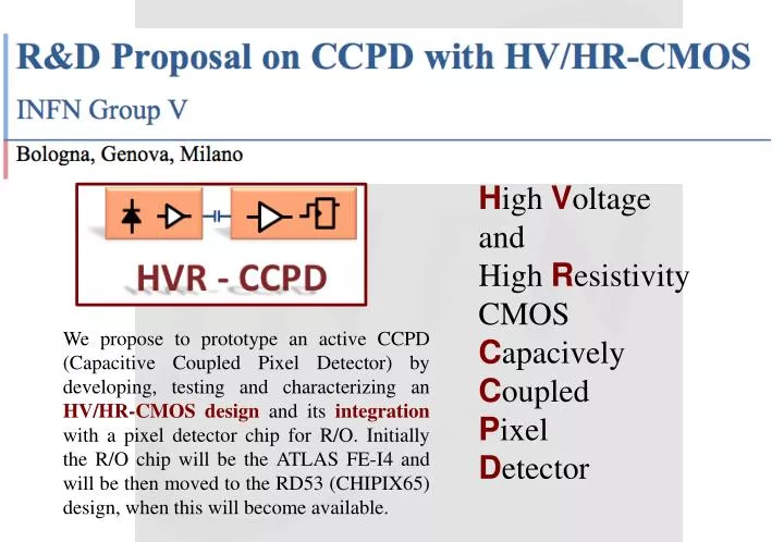
H igh V oltage and High R esistivity CMOS C apacively C oupled P ixel D etector.

E N D
High Voltage and High Resistivity CMOS Capacively Coupled Pixel Detector We propose to prototype an active CCPD (Capacitive Coupled Pixel Detector) by developing, testing and characterizing an HV/HR-CMOS design and its integration with a pixel detector chip for R/O. Initially the R/O chip will be the ATLAS FE-I4 and will be then moved to the RD53 (CHIPIX65) design, when this will become available.
HVR_CCPD: sensor A CMOS detector with a twist! • In standard CMOS detectors charge generated by energy deposition is collected by diffusion. • Combining commercial technologies sustaining HV (50-70 V) with high resistivity substrates results in a depleted (15-30 μm) region, where charge is collected by drift. • Same advantages of CMOS detectors (cheap, thin) • In addition: larger and faster signals and better radiation tolerance. • ST Microelectronics BCD8 technology has interesting features: • HV process at the 160 nm node: large scale production for power application (automotive) • Complete set of available devices (Bipolar, CMOS, D-MOS) • Epitaxial process (allow using different substrates) ST R&D group in AgrateBrianza is open to give access to their R&D runs for the development of these detectors. HVR_CCPD Proposal
HVR_CCPD: hybridization • High speed and high counting rate applications need complex logic and readout schemes: • not feasible in monolithic detectors • a readout chip is needed • Signal amplification on CMOS detectors allows AC coupling between the sensor and the readout chip: • alternative to bump-bonding process • significantly simpler and cheaper • independent from density of pixels • Small size CCPD prototypes have been assembled, • but no technology yet developed to guaranteeAC coupling uniformity on surfaces of detector size (few cm2). • Plan to develop a controlled flip-chip process: • growing of spacers in epoxy material (SU8) to control glue (dielectric) thickness • microfabrication capabilities in house (Low Temperature Detector laboratory) • characterization of coupling, uniformity, radiation tolerance in single dies • wafer level processing in external firms. HVR_CCPD Proposal
HVR_CCPD: manpower (resp. naz.) CMOS sensor Hybridization Characterization and test beams HVR_CCPD Proposal
HVR_CCPD: financial requests Hybridization process CMOS sensor production • Total request 309 k€ in 3 years. • 2/3 for CMOS sensor production • assume 1 submission/year • 1/3 for development of hybridization process • production of mechanical wafers • wafer level processing in external firms • Re-use front-end ASIC (FE-I4) and readout system from the ATLAS-IBL construction: • large saving on the costs (money and manpower) for the test systems • allows to join ATLAS upgrade irradiations and test beams HVR_CCPD Proposal