1 / 0

Transients and Step Responses

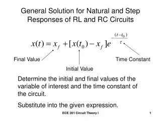
Transients and Step Responses. ELCT222- Lecture Notes University of S. Carolina Spring 2012. Outline. RC transients charging RC transients discharge RC transients Thevenin P-SPICE RL transients charging RL transients discharge Step responses. P-SPICE simulations Applications.

reba
Download Presentation

Transients and Step Responses

An Image/Link below is provided (as is) to download presentation Download Policy: Content on the Website is provided to you AS IS for your information and personal use and may not be sold / licensed / shared on other websites without getting consent from its author. Content is provided to you AS IS for your information and personal use only. Download presentation by click this link. While downloading, if for some reason you are not able to download a presentation, the publisher may have deleted the file from their server. During download, if you can't get a presentation, the file might be deleted by the publisher.

E N D

Presentation Transcript


  1. Transients and Step Responses

    ELCT222- Lecture Notes University of S. Carolina Spring 2012
  2. Outline RC transients charging RC transients discharge RC transients Thevenin P-SPICE RL transients charging RL transients discharge Step responses. P-SPICE simulations Applications Reading: Boylestad Sections 10.5, 10.6, 10.7, 10.9,10.10 24.1-24.7
  3. FIG. 10.26 Basic R-C charging network. TRANSIENTS IN CAPACITIVE NETWORKS: THE CHARGING PHASE The placement of charge on the plates of a capacitor does not occur instantaneously. Instead, it occurs over a period of time determined by the components of the network.
  4. FIG. 10.27 vC during the charging phase. TRANSIENTS IN CAPACITIVE NETWORKS: THE CHARGING PHASE
  5. FIG. 10.28 Universal time constant chart. TRANSIENTS IN CAPACITIVE NETWORKS: THE CHARGING PHASE
  6. TABLE 10.3 Selected values of e-x. TRANSIENTS IN CAPACITIVE NETWORKS: THE CHARGING PHASE
  7. TRANSIENTS IN CAPACITIVE NETWORKS: THE CHARGING PHASE The factor t, called the time constant of the network, has the units of time, as shown below using some of the basic equations introduced earlier in this text: The larger R is, the lower the charging current, longer time to charge The larger C is, the more charge required for a given V, longer time.
  8. FIG. 10.29 Plotting the equation yC =E(1 –e-t/t) versus time (t). TRANSIENTS IN CAPACITIVE NETWORKS: THE CHARGING PHASE
  9. TRANSIENTS IN CAPACITIVE NETWORKS: THE CHARGING PHASE
  10. FIG. 10.32 Revealing the short-circuit equivalent for the capacitor that occurs when the switch is first closed. TRANSIENTS IN CAPACITIVE NETWORKS: THE CHARGING PHASE
  11. FIG. 10.31 Demonstrating that a capacitor has the characteristics of an open circuit after the charging phase has passed. TRANSIENTS IN CAPACITIVE NETWORKS: THE CHARGING PHASE
  12. TRANSIENTS IN CAPACITIVE NETWORKS: THE CHARGING PHASE
  13. FIG. 10.34 Calculator key strokes to determine e-1.2. TRANSIENTS IN CAPACITIVE NETWORKS: THE CHARGING PHASEUsing the Calculator to Solve Exponential Functions
  14. FIG. 10.35 Transient network for Example 10.6. TRANSIENTS IN CAPACITIVE NETWORKS: THE CHARGING PHASEUsing the Calculator to Solve Exponential Functions Equation vC=E(1 –e-t/τ)
  15. FIG. 10.36 vC versus time for the charging network in Fig. 10.35. TRANSIENTS IN CAPACITIVE NETWORKS: THE CHARGING PHASEUsing the Calculator to Solve Exponential Functions
  16. FIG. 10.37 Plotting the waveform in Fig. 10.36 versus time (t). TRANSIENTS IN CAPACITIVE NETWORKS: THE CHARGING PHASEUsing the Calculator to Solve Exponential Functions
  17. FIG. 10.38 iC and yR for the charging network in Fig. 10.36. TRANSIENTS IN CAPACITIVE NETWORKS: THE CHARGING PHASEUsing the Calculator to Solve Exponential Functions
  18. TRANSIENTS IN CAPACITIVE NETWORKS: THE DISCHARGING PHASE We now investigate how to discharge a capacitor while exerting some control on how long the discharge time will be. You can, of course, place a lead directly across a capacitor to discharge it very quickly—and possibly cause a visible spark. For larger capacitors such those in TV sets, this procedure should not be attempted because of the high voltages involved—unless, of course, you are trained in the maneuver.
  19. FIG. 10.39 (a) Charging network; (b) discharging configuration. TRANSIENTS IN CAPACITIVE NETWORKS: THE DISCHARGING PHASE
  20. TRANSIENTS IN CAPACITIVE NETWORKS: THE DISCHARGING PHASE For the voltage across the capacitor that is decreasing with time, the mathematical expression is:
  21. FIG. 10.40 yC, iC, and yR for 5t switching between contacts in Fig. 10.39(a). TRANSIENTS IN CAPACITIVE NETWORKS: THE DISCHARGING PHASE
  22. FIG. 10.41 vC and iC for the network in Fig. 10.39(a) with the values in Example 10.6. TRANSIENTS IN CAPACITIVE NETWORKS: THE DISCHARGING PHASE
  23. TRANSIENTS IN CAPACITIVE NETWORKS: THE DISCHARGING PHASEThe Effect of on the Response
  24. FIG. 10.43 Effect of increasing values of C (with R constant) on the charging curve for vC. TRANSIENTS IN CAPACITIVE NETWORKS: THE DISCHARGING PHASEThe Effect of on the Response
  25. FIG. 10.44 Network to be analyzed in Example 10.8. TRANSIENTS IN CAPACITIVE NETWORKS: THE DISCHARGING PHASEThe Effect of on the Response
  26. FIG. 10.45 vC and iC for the network in Fig. 10.44. TRANSIENTS IN CAPACITIVE NETWORKS: THE DISCHARGING PHASEThe Effect of on the Response
  27. FIG. 10.46 Network to be analyzed in Example 10.9. FIG. 10.47 The charging phase for the network in Fig. 10.46. TRANSIENTS IN CAPACITIVE NETWORKS: THE DISCHARGING PHASEThe Effect of on the Response
  28. FIG. 10.48 Network in Fig. 10.47 when the switch is moved to position 2 at t =1t1. TRANSIENTS IN CAPACITIVE NETWORKS: THE DISCHARGING PHASEThe Effect of on the Response
  29. FIG. 10.49 vC for the network in Fig. 10.47. TRANSIENTS IN CAPACITIVE NETWORKS: THE DISCHARGING PHASEThe Effect of on the Response
  30. FIG. 10.50 ic for the network in Fig. 10.47. TRANSIENTS IN CAPACITIVE NETWORKS: THE DISCHARGING PHASEThe Effect of on the Response
  31. FIG. 10.51 Defining the regions associated with a transient response. INITIAL CONDITIONS The voltage across the capacitor at this instant is called the initial value, as shown for the general waveform in Fig. 10.51.
  32. FIG. 10.52 Example 10.10. INITIAL CONDITIONS
  33. FIG. 10.53 vC and iC for the network in Fig. 10.52. INITIAL CONDITIONS
  34. FIG. 10.54 Defining the parameters in Eq. (10.21) for the discharge phase. INITIAL CONDITIONS
  35. FIG. 10.55 Key strokes to determine (2 ms)(loge2) using the TI-89 calculator. INSTANTANEOUS VALUES Occasionally, you may need to determine the voltage or current at a particular instant of time that is not an integral multiple of t.
  36. THÉVENIN EQUIVALENT: t =RThC You may encounter instances in which the network does not have the simple series form in Fig. 10.26. You then need to find the Thévenin equivalent circuit for the network external to the capacitive element.
  37. FIG. 10.56 Example 10.11. THÉVENIN EQUIVALENT: t =RThC
  38. FIG. 10.57 Applying Thévenin’s theorem to the network in Fig. 10.56. THÉVENIN EQUIVALENT: t =RThC
  39. FIG. 10.58 Substituting the Thévenin equivalent for the network in Fig. 10.56. THÉVENIN EQUIVALENT: t =RThC
  40. FIG. 10.59 The resulting waveforms for the network in Fig. 10.56. THÉVENIN EQUIVALENT: t =RThC
  41. FIG. 10.61 Network in Fig. 10.60 redrawn. FIG. 10.60 Example 10.12. THÉVENIN EQUIVALENT: t =RThC
  42. FIG. 10.62 yC for the network in Fig. 10.60. THÉVENIN EQUIVALENT: t =RThC
  43. FIG. 10.63 Example 10.13. THÉVENIN EQUIVALENT: t =RThC
  44. THE CURRENT iC There is a very special relationship between the current of a capacitor and the voltage across it. For the resistor, it is defined by Ohm’s law: iR = vR/R. The current through and the voltage across the resistor are related by a constant R—a very simple direct linear relationship. For the capacitor, it is the more complex relationship defined by:
  45. FIG. 10.64 vC for Example 10.14. THE CURRENT iC
  46. FIG. 10.65 The resulting current iC for the applied voltage in Fig. 10.64. THE CURRENT iC
  47. Inductors

  48. R-L TRANSIENTS: THE STORAGE PHASE The storage waveforms have the same shape, and time constants are defined for each configuration. Because these concepts are so similar (refer to Section 10.5 on the charging of a capacitor), you have an opportunity to reinforce concepts introduced earlier and still learn more about the behavior of inductive elements.
  49. FIG. 11.31 Basic R-L transient network. R-L TRANSIENTS: THE STORAGE PHASE Remember, for an inductor
  50. FIG. 11.32 iL, yL, and yR for the circuit in Fig. 11.31 following the closing of the switch. R-L TRANSIENTS: THE STORAGE PHASE
  51. FIG. 11.33 Effect of L on the shape of the iL storage waveform. R-L TRANSIENTS: THE STORAGE PHASE
  52. FIG. 11.34 Circuit in Figure 11.31 the instant the switch is closed. R-L TRANSIENTS: THE STORAGE PHASE
  53. FIG. 11.36 Series R-L circuit for Example 11.3. FIG. 11.35 Circuit in Fig. 11.31 under steady-state conditions. R-L TRANSIENTS: THE STORAGE PHASE
  54. R-L TRANSIENTS: THE STORAGE PHASE FIG. 11.37 iL and vL for the network in Fig. 11.36.
  55. INITIAL CONDITIONS Since the current through a coil cannot change instantaneously, the current through a coil begins the transient phase at the initial value established by the network (note Fig. 11.38) before the switch was closed. It then passes through the transient phase until it reaches the steady-state (or final) level after about five time constants. The steadystate level of the inductor current can be found by substituting its shortcircuit equivalent (or Rlfor the practical equivalent) and finding the resulting current through the element.
  56. FIG. 11.38 Defining the three phases of a transient waveform. INITIAL CONDITIONS
  57. FIG. 11.39 Example 11.4. INITIAL CONDITIONS
  58. FIG. 11.40 iL and vL for the network in Fig. 11.39. INITIAL CONDITIONS
  59. FIG. 11.41 Demonstrating the effect of opening a switch in series with an inductor with a steady-state current. R-L TRANSIENTS: THE RELEASE PHASE
  60. FIG. 11.42 Initiating the storage phase for an inductor by closing the switch. R-L TRANSIENTS: THE RELEASE PHASE
  61. FIG. 11.43 Network in Fig. 11.42 the instant the switch is opened. R-L TRANSIENTS: THE RELEASE PHASE
  62. R-L TRANSIENTS: THE RELEASE PHASE
  63. FIG. 11.45 The various voltages and the current for the network in Fig. 11.44. R-L TRANSIENTS: THE RELEASE PHASE
  64. Step Responses

  65. OBJECTIVES Become familiar with the specific terms that define a pulse waveform and how to calculate various parameters such as the pulse width, rise and fall times, and tilt. Be able to calculate the pulse repetition rate and the duty cycle of any pulse waveform. Become aware of the parameters that define the response of an R-C network to a square-wave input. Understand how a compensator probe of an oscilloscope is used to improve the appearance of an output pulse waveform.
  66. FIG. 24.1 Ideal pulse waveform. IDEAL VERSUS ACTUAL The ideal pulse in Fig. 24.1 has vertical sides, sharp corners, and a flat peak characteristic; it starts instantaneously at t1 and ends just as abruptly at t2.
  67. FIG. 24.2 Actual pulse waveform. IDEAL VERSUS ACTUAL
  68. IDEAL VERSUS ACTUAL Amplitude Pulse Width Base-Line Voltage Positive-Going and Negative-Going Pulses Rise Time (tr) and Fall Time (tf) Tilt
  69. FIG. 24.3 Defining the base-line voltage. IDEAL VERSUS ACTUAL
  70. FIG. 24.4 Positive-going pulse. IDEAL VERSUS ACTUAL
  71. FIG. 24.5 Defining tr and tf. IDEAL VERSUS ACTUAL
  72. FIG. 24.6 Defining tilt. IDEAL VERSUS ACTUAL
  73. FIG. 24.7 Defining preshoot, overshoot, and ringing. IDEAL VERSUS ACTUAL
  74. FIG. 24.8 Example 24.1. IDEAL VERSUS ACTUAL
  75. FIG. 24.9 Example 24.2. IDEAL VERSUS ACTUAL
  76. PULSE REPETITION RATE AND DUTY CYCLE A series of pulses such as those appearing in Fig. 24.10 is called a pulse train. The varying widths and heights may contain information that can be decoded at the receiving end. If the pattern repeats itself in a periodic manner as shown in Fig. 24.11(a) and (b), the result is called a periodic pulse train.
  77. FIG. 24.11 Periodic pulse trains. PULSE REPETITION RATE AND DUTY CYCLE
  78. FIG. 24.12 Example 24.3. PULSE REPETITION RATE AND DUTY CYCLE
  79. FIG. 24.13 Example 24.4. PULSE REPETITION RATE AND DUTY CYCLE
  80. FIG. 24.14 Example 24.5. PULSE REPETITION RATE AND DUTY CYCLE
  81. AVERAGE VALUE The average value of a pulse waveform can be determined using one of two methods. The first is the procedure outlined in Section 13.7, which can be applied to any alternating waveform. The second can be applied only to pulse waveforms since it utilizes terms specifically related to pulse waveforms; that is,
  82. FIG. 24.15 Example 24.6. AVERAGE VALUE
  83. FIG. 24.16 Solution to part (b) of Example 24.7. AVERAGE VALUE
  84. FIG. 24.17 Determining the average value of a pulse waveform using an oscilloscope. AVERAGE VALUEInstrumentation The average value (dc value) of any waveform can be easily determined using the oscilloscope. If the mode switch of the scope is set in the ac position, the average or dc component of the applied waveform is blocked by an internal capacitor from reaching the screen.
  85. TRANSIENT R-C NETWORKS In Chapter 10, the general solution for the transient behavior of an R-C network with or without initial values was developed. The resulting equation for the voltage across a capacitor is repeated here for convenience:
  86. FIG. 24.18 Defining the parameters of Eq. (24.6). TRANSIENT R-C NETWORKS
  87. FIG. 24.19 Example of the use of Eq. (24.6). TRANSIENT R-C NETWORKS
  88. FIG. 24.20 Example 24.8. TRANSIENT R-C NETWORKS
  89. FIG. 24.21 yC and iC for the network in Fig. 24.20. TRANSIENT R-C NETWORKS
  90. FIG. 24.22 Example 24.9. TRANSIENT R-C NETWORKS
  91. FIG. 24.23 vC for the network in Fig. 24.22. TRANSIENT R-C NETWORKS
  92. FIG. 24.24 Periodic square wave. R-C RESPONSE TO SQUARE-WAVE INPUTS The square wave in Fig. 24.24 is a particular form of pulse waveform. It has a duty cycle of 50% and an average value of zero volts, as calculated as follows:
  93. FIG. 24.25 Raising the base-line voltage of a square wave to zero volts. R-C RESPONSE TO SQUARE-WAVE INPUTS
  94. FIG. 24.26 Applying a periodic square-wave pulse train to an R-C network. R-C RESPONSE TO SQUARE-WAVE INPUTS
  95. T/2 > 5t
  96. T/2 = 5t
  97. T/2 <5T
  98. FIG. 24.30 vC for T/2 << 5t or T << 10t. T/2 <5T
  99. FIG. 24.31 Example 24.10. R-C RESPONSE TO SQUARE-WAVE INPUTS
  100. FIG. 24.32 vC for the R-C network in Fig. 24.31. R-C RESPONSE TO SQUARE-WAVE INPUTS
  101. FIG. 24.33 iC for the R-C network in Fig. 24.31. R-C RESPONSE TO SQUARE-WAVE INPUTS
  102. R-C RESPONSE TO SQUARE-WAVE INPUTS
  103. R-C RESPONSE TO SQUARE-WAVE INPUTS
  104. OSCILLOSCOPE ATTENUATOR AND COMPENSATING PROBE The X10 attenuator probe used with oscilloscopes is designed to reduce the magnitude of the input voltage by a factor of 10. If the input impedance to a scope is 1 MΩ, the X10 attenuator probe will have an internal resistance of 9 MΩ, as shown in Fig. 24.36.
  105. FIG. 24.36 X10 attenuator probe. OSCILLOSCOPE ATTENUATOR AND COMPENSATING PROBE
  106. FIG. 24.37 Capacitive elements present in an attenuator probe arrangement. OSCILLOSCOPE ATTENUATOR AND COMPENSATING PROBE
  107. FIG. 24.38 Equivalent network in Fig. 24.37. OSCILLOSCOPE ATTENUATOR AND COMPENSATING PROBE
  108. FIG. 24.39 Thévenin equivalent for Ci in Fig. 24.38. OSCILLOSCOPE ATTENUATOR AND COMPENSATING PROBE
  109. FIG. 24.40 The scope pattern for the conditions in Fig. 24.38 with vt = 200 V peak. OSCILLOSCOPE ATTENUATOR AND COMPENSATING PROBE
  110. FIG. 24.41 Commercial compensated 10 : 1 attenuator probe. (Courtesy of Tektronix, Inc.) OSCILLOSCOPE ATTENUATOR AND COMPENSATING PROBE
  111. FIG. 24.42 Compensated attenuator and input impedance to a scope, including the cable capacitance. OSCILLOSCOPE ATTENUATOR AND COMPENSATING PROBE
More Related