Download
1 / 35
360 likes | 442 Views
The CMOS Inverter. Lecture 3 Static properties = voltage transfer curves (VTC) and noise margins. Week 2: The CMOS inverter. Tuesday Static properties Voltage transfer curves (VTC) Noise margins Exercise ( Kjell , 1 hour) Thursday Dynamic properties Propagation delay

E N D
The CMOS Inverter Lecture 3 Staticproperties = voltage transfer curves (VTC) and noisemargins
Week 2: The CMOS inverter • Tuesday • Static properties • Voltage transfer curves (VTC) • Noise margins • Exercise (Kjell, 1 hour) • Thursday • Dynamic properties • Propagation delay • Driving large capacitive loads w. optimal propagation delay • Exercise POTW (Victor, 2 hours) • Friday • Prelab 1 deadline 1PM MCC092 IC Design - Lecture 3: The Inverter
What happened last week? • Let’s do a quiz about the transistor: • Go to socrative.com • Select Student login • Go to room: “MCC0922018” MCC092 IC Design - Lecture 3: The Inverter
Where are we? Inverter Logic gates P-type pull-up network P OUT OUT IN IN N-type Pull-down network N Designing w switches Hands-on lab session MCC092 IC Design - Lecture 3: The Inverter
Where are we? Inverter Logic gates P-type pull-up network 0 OUT 1 IN N-type Pull-down network Designing w switches Hands-on lab session MCC092 IC Design - Lecture 3: The Inverter
Where are we? Inverter Logic gates P-type pull-up network 1 OUT 0 IN N-type Pull-down network Designing w switches Hands-on lab session MCC092 IC Design - Lecture 3: The Inverter
Where are we? Inverter Logic gates P-type pull-up network IDS VSW OUT VSW IN N-type Pull-down network Designing w switches Hands-on lab session MCC092 IC Design - Lecture 3: The Inverter
MOSFET I/V Characteristics IDS Saturation: IDSN=IDSAT,N ON • IDSN=GONVDS VDS OFF: IDS=0 OFF: IDS=0 • IDSP=GONVDS Saturation: IDSP=IDSAT,P ON MCC092 IC Design - Lecture 3: The Inverter
MOSFET I/V Characteristics IDS Saturation: IDSN=IDSAT,N ON Saturation: ISDP=IDSAT,P ON • ISDP=GONVSD • IDSN=GONVDS VDS OFF: IDS=0 OFF: IDS=0 MCC092 IC Design - Lecture 3: The Inverter
MOSFET I/V Characteristics IDS Saturation: IDSN=IDSAT,N ON Saturation: IDSP=IDSAT,P • IDSN=GONVDS VDS OFF: IDS=0 MCC092 IC Design - Lecture 3: The Inverter
VIN/VOUT voltage plane VOUT VDD, VDD VDD NMOS NMOS OFF VIN VDD PMOS PMOS OFF MCC092 IC Design - Lecture 3: The Inverter
VIN/VOUT voltage plane VOUT VDD, VDD VDD NMOS OFF PMOS OFF VIN VDD MCC092 IC Design - Lecture 3: The Inverter
Voltage Transfer Characteristic - VTC VOUT VDD, VDD Inverter IDS VDD • IDS,P=0 NMOS OFF PMOS OFF 1 0 • IDS,N=0 VIN VDD VDS The ON p-switch pulls the output high MCC092 IC Design - Lecture 3: The Inverter
Voltage Transfer Characteristic - VTC Inverter VOUT VDD, VDD VDD • IDS,P=0 0 1 NMOS OFF PMOS OFF • IDS,N=0 IDS VIN VDD The ON n-switch pulls the output low VDS MCC092 IC Design - Lecture 3: The Inverter
An aside about MOSFET current equations Shockley’s continuous model: Our piecewise linear model: MCC092 IC Design - Lecture 3: The Inverter
So with piecewise linear MOS model the inverter diagram is this: Notice different slopes between green and blue regions! Transition voltage is VGT/2 rather than VGT MCC092 IC Design - Lecture 3: The Inverter
Voltage Transfer Characteristic - VTC VOUT VDD, VDD Inverter VDD NMOS OFF PMOS OFF IDS VSW VSW IDS VIN VDD The ON n-switch pulls the output low VDS MCC092 IC Design - Lecture 3: The Inverter
Voltage Transfer Characteristic - VTC VOUT VDD, VDD Inverter VSW IDS VDD NMOS OFF PMOS OFF Switching means: VIN=VOUT IDS VSW VSW Saturation: IDSP,N=IDSAT,P VIN VDD VDS Switching occurs in the green region where both MOSFETs are saturated . . . . . . and saturation currents are equal: Solving for VINusing x=kN/kP yields MCC092 IC Design - Lecture 3: The Inverter
Voltage Transfer Characteristic - VTC DV VOUT Inverter VSW IDS VDD NMOS OFF PMOS OFF IDS VSW VSW Saturation: IDSP,N=IDSAT,P VIN VDD The switchingvoltageequation can be rewritten on a form easier to graspifweintroduce VDS MCC092 IC Design - Lecture 3: The Inverter
Voltage Transfer Characteristic - VTC VOUT VDD, VDD Inverter VSW IDS VDD NMOS OFF PMOS OFF IDS VSW VSW VIN VDD VDS Equal currents in top blue region where p-MOSFET is in linear region yields VOUT vs. VIN! MCC092 IC Design - Lecture 3: The Inverter
Voltage Transfer Characteristic - VTC VOUT VDD, VDD Inverter VSW IDS VDD NMOS OFF PMOS OFF IDS VSW VSW VIN VDD VDS Equal currents in bottom blue region where n-MOSFET is linear region yields VOUT vs. VIN! MCC092 IC Design - Lecture 3: The Inverter
The voltage characteristic (VTC) VOUT For x=kN/kP=1 we have What if we make n-channel MOSFET wider, i.e. for x>1? VDD What happens to VTC? WillswitchingvoltageVSW increase or decrease? Assume x=4 and we have Assumex=1/4 and we have 0 VIN VSW 0 VTN VDD+VTP VDD MCC092 IC Design - Lecture 3: The Inverter
The voltage characteristic (VTC) VOUT Which VTC is NAND and which VTC is NOR? Assumeall transistor same width VDD NAND NOR 0 VIN VSW 0 VTN VDD+VTP VDD MCC092 IC Design - Lecture 3: The Inverter
The voltage characteristic (VTC) VOUT How about current flow? No current flow in red regions! ”short-circuit” current ISCflows in blue/green regions n-channel MOSFET saturated for VIN<VSW VDD p-channel MOSFET saturated for VIN>VSW 0 VIN VSW 0 VTN VDD+VTP VDD MCC092 IC Design - Lecture 3: The Inverter
Noise margins • What are they? • Why are they important? Answers the question: How much noise can the circuit tolerate? MCC092 IC Design - Lecture 3: The Inverter
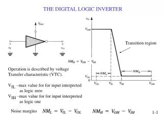
NoiseMargins - preliminairies VOUT Let´sdefine valid input and output voltage regions from pointswhereslopeof VTC is -1; That is whereAV = -1! AV is the voltagegain. VDD VOH,min Valid ”1” VOL,max Valid ”0” 0 0 VIL,max VIH,min VDD VIN MCC092 IC Design - Lecture 3: The Inverter
Noisemargins - NMH VOUT VDD VIN VDD Valid ”1” VOH,min NMH VIH,min VIN not valid Valid ”0” Valid ”1” VIL,max VOL,max Valid ”0” 0 VIN VIL,max VIH,min VOUT MCC092 IC Design - Lecture 3: The Inverter
Noise Margins- NML VOUT VDD VIN VDD Valid ”1” VOH,min VIH,min VIN not valid Valid ”1” VIL,max NML VOL,max Valid ”0” 0 VIN 0 VIH,min VIL,max VOUT MCC092 IC Design - Lecture 3: The Inverter
Regenerative effect = How well the signal is regenerated from input to output f(VIN) Consider a pair of cross-coupled inverters VIN VOUT that is g(VOUT) We take the partial derivate of this function w.r.t VIN (using the chain rule): Slopes, that is, small-signal gains So we see that the inverse of f (the VTC) is g in each pair of corresponding voltage points. Only if the VTC has a region of gain magnitude > 1 bordered by two regions of gain magnitude < 1 is the circuit regenerative. Then there are two stable operating points. The VTC and its inverse are illustrated in the butterfly diagram. MCC092 IC Design - Lecture 3: The Inverter
Butterfly Diagram In each pair of corresponding voltage points (VIN, VOUT) the product of the derivatives (that is the small-signal gains) of the two curves is 1 The points where both gains are -1 defines the voltages of interest for noise margins VOUT VDD VIN VOUT Valid ”1” VOH,min Memory cell characterization NMH VTC, that is f Inverse of VTC, that is g NML See W&H section 12.2.1.3 for more info if you want to. VOL,max Valid ”0” 0 VIN 0 VIH,min VIL,max MCC092 IC Design - Lecture 3: The Inverter
Noise Margins – skewed inverters NMH NML NML NMH MCC092 IC Design - Lecture 3: The Inverter
Noise Margins – an example NMH=VOH,min-VIH,minNML=VIL,max-VOL,max Let´sdefine valid regions from points where slope AV = -1! VOUT Thesepointsyieldsnumbers for (VOH,min, VIL,max) and (VOL,max, VIH,min) so that NMH and NML can be calculated! VDD Valid ”1” VOH,min VOL,max Valid ”0” 0 VIN 0 VIL,max VIH,min VDD MCC092 IC Design - Lecture 3: The Inverter
Noise Margins – an example NMH=VOH,min-VIH,min1.12-0.68=0.44 VNML=VIL,max- VOL,max = 0.52-0.08=0.44 V NMH=VOH,min-VIH,minNML=VIL,max-VOL,max Let´sdefine valid regions from points where slope AV = -1! VOUT DV=0.64 V 0.28 V 0.28 V Thesepointsyieldsnumbers for (VOH,min, VIL,max) and (VOL,max, VIH,min) so that NMH and NML can be calculated! VDD Valid ”1” DV/8 VOH,min For x=1, VTN=0.28 V and VTP=-0.28 V wehaveVSW=0.28+0.64/2=0.60 V and DV=0.64 V DV/8 DV/8 Formulas can be derived (for x=1):VOH,min=VDD-DV/8VOL,max = DV/8 VIL,max=VSW-DV/8 VIH,min=VSW+DV/8 Formulas can be derived (for x=1): VOH,min=VDD-DV/8=1.12 VVOL,max = DV/8=80 mV VIL,max=VSW-DV/8=0.52 V VIH,min=VSW+DV/8=0.68 V VDD = 1.2 V VOL,max DV/8 Valid ”0” 0 VIN 0 VIL,max VIH,min VDD MCC092 IC Design - Lecture 3: The Inverter
What about lab 1 • Calculate VSW and find from simulation in lab • Calculate noise margins and find from simulation MCC092 IC Design - Lecture 3: The Inverter
Summary • CMOS inverter – schematic • Voltage transfer characteristics (VTC) • Regions of operation • How to calculateswitching voltage VSW • VSW dependence on kN/kP(that is, transistor widths) • Understand switching current (ISC) flow • Noisemargins: NMH and NML • Whyimportant? • Definition • Butterfly diagram MCC092 IC Design - Lecture 3: The Inverter