Download
1 / 29
390 likes | 664 Views
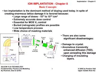
Chapter 8 Ion Implantation. ION IMPLANTATION SYSTEM. Ion implanter is a high-voltage accelerator of high-energy impurity ions Major components are: Ion source (gases such as AsH 3 , PH 3 , B 2 H 6 ) Mass Spectrometer (selects the ion of interest) HV Accelerator (voltage > 1 MeV)

E N D
ION IMPLANTATION SYSTEM • Ion implanter is a high-voltage accelerator of high-energy impurity ions • Major components are: • Ion source (gases such as AsH3 , PH3 , B2H6) • Mass Spectrometer (selects the ion of interest) • HV Accelerator (voltage > 1 MeV) • Scanning System (x-y deflection plates for electronic control) • Target Chamber (vacuum)
0 to 175 kV Neutral beam trap and beam gate R R R Beam trap Neutral beam C C C Resolving aperture 2 Integrator 90o analyzing magnet Q 3 Focus Acceleration tube 5 y-axis scanner Ion source x-axis scanner 1 4 25 kV Wafer in process chamber ION IMPLANTATION SYSTEM • Cross-section of an ion implanter m/q=(B2R2)/(2V) Or Faraday cup Acceleration energy = voltage x charge on ion
http://www.bpc.edu/mathscience/chemistry/images/periodic_table_of_elements.jpghttp://www.bpc.edu/mathscience/chemistry/images/periodic_table_of_elements.jpg
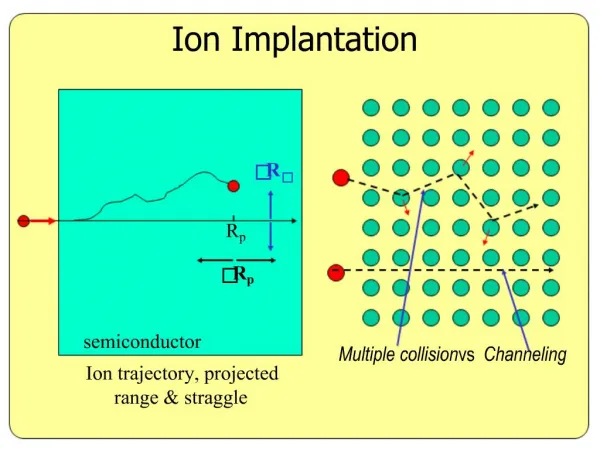
ION IMPLANTATION • High energy ion enters crystal lattice and collides with atoms and interacts with electrons • Types of collisions: Nuclear and electron • Each collision or interaction reduces energy of ion until it comes to rest • Amount of energy loss is dependent on ion, the energy it has at the time of the scattering event, and the type of scattering.
From Handbook of Semiconductor Manufacturing Technology by Yoshio Nishi and Robert Doering
From Handbook of Semiconductor Manufacturing Technology by Yoshio Nishi and Robert Doering
Channeling • Deep penetration by the ion because it traveled along a path where no semiconductor atoms are situated • Process is used for materials characterization: Rutherford backscattering • To prevent channeling • Implantation is performed at an angle of about 8° off the normal to the wafer surface. • The wafer surface is amorphorized by a high dose, low energy implantation of a nonelectrically active ion. • Hydrogen, helium, and silicon are common ions used
Determining the Dose • The implanted dose can be accurately measured by monitoring the ion beam current using a Faraday cup • The integrated current during the implant divided by the charge on the ion is the dose.
Post Implantation Anneals • An annealing step is required to repair crystal damage (recrystallization) and to electrically activated the dopants. • Dislocations will form during the anneal so times and temperatures must be chosen to force dislocations disappear. • If the anneal time is long and the temperature is high, a drive of the implanted ions may occur.
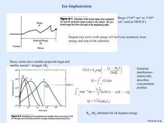
ION IMPLANTATION • Projected range (RP): the average distance an ion travels before it stops. • Projected straggle (RP): deviation from the projected range due to multiple collisions. http://eserver.bell.ac.uk
MODEL FOR ION IMPLANTATION • Distribution is Gaussian Cp = peak concentration Rp = range Rp = straggle
MODEL FOR ION IMPLANTATION • For an implant contained within silicon, the dose is
ION IMPLANTATION MODEL • Model developed by Lindhard, Scharff and Schiott (LSS) • Range and straggle roughly proportional to energy over wide range • Ranges in Si and SiO2 roughly the same • Computer models now available
1.0 B P As Sb Projected range (mm) 0.1 Rp 0.01 1000 10 100 Acceleration energy (keV) Range of impurities in Si
0.10 Sb B Normal and transverse straggle (mm) P 0.01 As DRp DR 0.002 10 1000 100 Acceleration energy (keV) Straggle of impurities in Si
Si SiO2 AZ-7500 resist Si3N4 http://www.iue.tuwien.ac.at/phd/hoessinger/node22.html
SiO2 AS A BARRIER • The minimum oxide thickness for selective implantation: Xox = RP + RP (2 ln(10CP/CBulk))0.5 • An oxide thickness equal to the projected range plus six times the straggle should mask most ion implants.
Other Materials • A silicon nitride barrier layer needs only be 85% of the thickness of an oxide barrier layer. • A photoresist barrier must be 1.8 times the thickness of an oxide layer under the same implantation conditions. • Metals are of such a high density that even a very thin layer will mask most implantations. • Nickel is one of the most commonly used metal masks
ADVANTAGES • Low temperature process • The wafer is cooled from the backside during high energy, high current diffusions are performed • Less change of stress-induced dislocations due to thermal expansion issues • Wider range of barrier materials • Photoresist • Wider range of impurities • No concern about solid solubility limitations • Implantation of ions such as oxygen, hydrogen, helium, and other ions with low solid solubility is possible.
Advantages over Diffusion • Better control and wider range of dose compared to predep diffusions • Impurity concentration profile controlled by accelerating voltage • Very shallow layers • Lateral scattering effects are smaller than lateral diffusion.
FINAL PROFILE 15 200 KILOELECTRON VOLTS 100 10 NITROGEN CONCENTRATION (ATOMIC PERCENT) 50 20 10 5 0 0 50 100 150 200 250 350 300 DEPTH (NANOMETERS) • Complex-doping profiles can be produced by superimposing multiple implants having various ion energies and doses.
RADIATION DAMAGE • Impact of incident ions knocks atoms off lattice sites • With sufficient dose, can make amorphous Si layer
Critical dose to make layer amorphous varies with temperature and impurity 1018 1017 1016 Critical dose (atom/cm2) B 1015 P Sb 1014 1013 0 1 2 3 4 5 6 7 8 9 10 Temperature, 1000/T (K-1) RADIATION DAMAGE
Recrystallization • Radiation damage can be removed by annealing at 800-1000oC for 30 min. After annealing, a significant percentage of the impurities become electronically active. • Point defects coalesce into line dislocations • Line dislocations merge into loop dislocations • Loop dislocations slowly disintegrate as interstitial Si atoms move on to lattice sites
Implanting through a sacrificial oxide layer: Large ions (arsenic) can be slowed down a little before penetrating into the silicon. The crystal lattice damage is suppressed (at the expense of the depth achieved). Collisions with the thin masking layer tends to cause the dopant ions to change direction randomly, thereby suppressing channeling effect. The concentration peak can be brought closer to the silicon surface. Ion Implantation
Ion Implantation • For deep diffusion (>1µm), implantation is used to introduce a certain dose, and thermal diffusion is used to drive in the dopants. • The resulting profile after diffusion can be determined by: