Download
1 / 18
180 likes | 330 Views
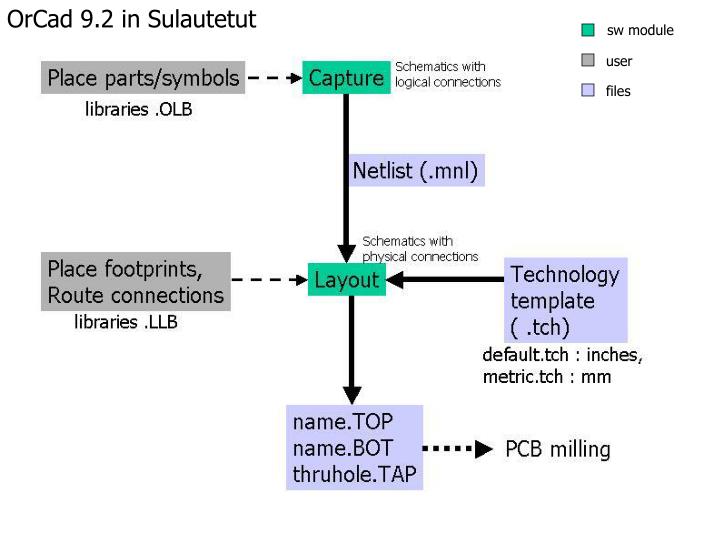
OrCad 9.2 in Sulautetut. sw module. user. files. Capture. Start Cadence PSD 14.0 Capture. Schematics, logical connections. File Open Project h8s_eval.opj Open. Example H8S_evalBoard.zip can be downloaded from :. http://www.ee.oulu.fi/~ terva / Embedded2003 / bulletin.php.

E N D
OrCad 9.2 in Sulautetut sw module user files
Capture Start Cadence PSD 14.0 Capture Schematics, logical connections File Open Project h8s_eval.opj Open Example H8S_evalBoard.zipcan be downloaded from : http://www.ee.oulu.fi/~terva/Embedded2003/bulletin.php File Save As name.opj Save As change the name of the project. Link to HW manual of the MCU is at: http://www.ee.oulu.fi/~hannu/Embedded2003/mcus.php
Overview Design pages Offpage connector Microcontroller H8S2128 GND (0v) Library of symbols VCC (+5v)
Place a part e.g a DB9 connector (for serial communication) Place Part in the Libraries field, select Sulautetut2 , in the Part List field, select DB9S , then Click OK . To rotate a part : Select a part (left click on the part) , CTRL-R . Place a wire Place Wire , Use the mouse to draw the wire. Place an offpage connector to connect 2 pins that are on different design pages, ! Give the same name on each of the pages, for one connection.
Toolbar for wires, parts, GND, VCC, offpage connectors ...
Design Rule check : unconnected nets, off-page connectors Tools Design Rule Check Nota: menu Tools is visible only when a design page is selected.
Create a netlist (.MNL) Tools Create Netlist Check the report messages in the Session Log window. Automatic update CaptureLayout
Layout Bottom/Top layer view Pad : Copper Copper (kupari) Insulation (eristys) Padstack : list of those dimensions for one pad. Hole (reikä) Top layer Bottom layer if copper on the interior of this cylinder : pad is also via (the current flows between layers). Footprint : padstack(s) + obstacle(s)
Start Cadence PSD 14.0 Layout • File New • Default.tch / Metric.tch (inches/mm). • then automatically, Layout asks the netlist file (.MNL) , • next the name of the main output file (.MAX) • next the footprints of the components. .../... Use the library EVALBOARD.LLB for the main components; some footprints are missing, like the crystal resonator (Take e.g., a capa footprint. The crystal is not needed when using the emulator).
Link footprints EVALBOARD library
System settings : units Options System Settings
Spacing between items: used as routing rules. Options Global Spacing
Layers : 3 layers of interest Tools Layers Select from Spreadsheet
Nets selections/settings : Tools Nets Select from Spreadsheet Select one or several net names ,and a pop-up menu (right click) allows modifying the properties.
Create the board outline (ToolObstacleSelect Tool) Note Online DRC OFF Place components (footprints) For all modules Enable a modular group of nets (e.g LCD_Connec) Note Online DRC ON Route those nets (e.g. autoroute) Check out statistics of unrouted nets Cleanup design/Design Rule Check Create Reports Run Post Processor name.bot, name.top, thruhole.tap
Autorouting/Manual Route : • Auto AutoRoute Board : autorouting • Tool Track Select Tool , then use the mouse and right button (select Finish in the pop-up to terminate a track). Cleanup design/Design Rule Check : • Auto Cleanup Design • Select All, and Check Detail Obstacle. • Auto Design Rule Check • Select All, and Check Detail Obstacle. Check statistics of unrouted nets : • Auto Refresh Calculate Statistics • Check out the unrouted nets section. Create Reports : in order to see the location of unrouted nets. • Auto Create reports • Check the ”Conns Unrouted” box.
More detailed description of the previous steps : • http://www.ee.oulu.fi/~terva/Embedded2003/bulletin.php • on ”Intro to Orcad” link. • Even better description in the tutorial/help provided in the software. • Re-use the proposed example, the pad-to-pad spacing, and other properties/settings have been tested. • The design is quite simple : two layers TOP and BOT. THRUHOLE.TAP contains drilling properties/settings.
Via Text on top layer Obstacle