Download
1 / 1
30 likes | 186 Views
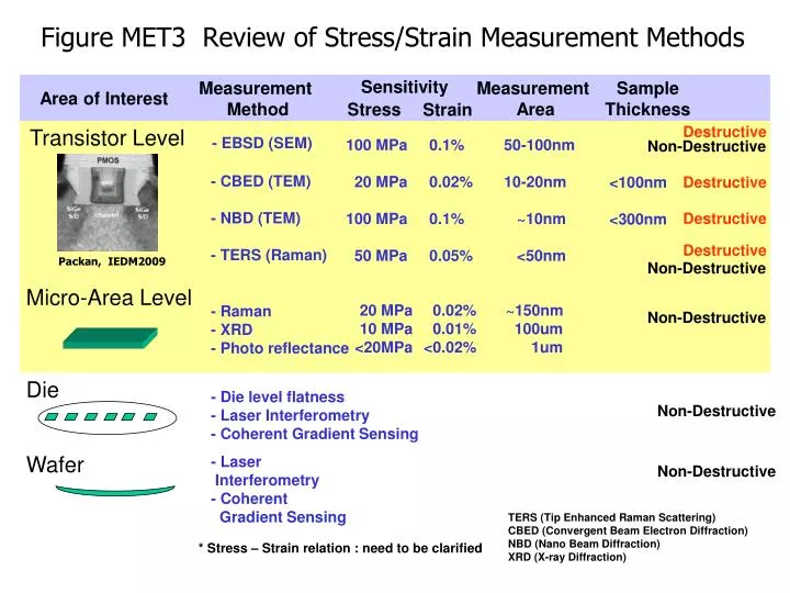
Figure MET3 Review of Stress/Strain Measurement Methods. Sensitivity. Measurement Method. Measurement Area. Sample Thickness. Area of Interest. Stress. Strain. Destructive. Transistor Level. - EBSD (SEM). 100 MPa 20 MPa 100 MPa 50 MPa. 0.1% 0.02% 0.1% 0.05%. 50-100nm

E N D
Figure MET3 Review of Stress/Strain Measurement Methods Sensitivity Measurement Method Measurement Area Sample Thickness Area of Interest Stress Strain Destructive Transistor Level - EBSD (SEM) 100 MPa 20 MPa 100 MPa 50 MPa 0.1% 0.02% 0.1% 0.05% 50-100nm 10-20nm ~10nm <50nm Non-Destructive - CBED (TEM) - NBD (TEM) - TERS (Raman) <100nm <300nm Destructive Destructive Destructive Packan, IEDM2009 Non-Destructive Micro-Area Level 20MPa 10 MPa <20MPa 0.02% 0.01% <0.02% ~150nm 100um 1um - Raman - XRD - Photo reflectance Non-Destructive Die - Die level flatness - Laser Interferometry - Coherent Gradient Sensing Non-Destructive Wafer - Laser Interferometry - Coherent Gradient Sensing Non-Destructive TERS (Tip Enhanced Raman Scattering) CBED (Convergent Beam Electron Diffraction) NBD (Nano Beam Diffraction) XRD (X-ray Diffraction) * Stress – Strain relation : need to be clarified