Download
1 / 41
410 likes | 423 Views
Universiti Malaysia Perlis. ENT356 INSTRUMENTATION SYSTEM. Lecture 6.1: Computer Data Acquisition System. General Computer DAQ System. Transducer. Signal Conditioning. A/D Conversion. Computer.

E N D
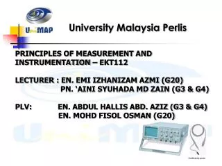
Universiti Malaysia Perlis ENT356 INSTRUMENTATION SYSTEM Lecture 6.1: Computer Data Acquisition System Sem 2, 2010/2011
General Computer DAQ System Transducer Signal Conditioning A/D Conversion Computer Sem 2, 2010/2011
A data acquisition (DAQ) system is a collection of add-on hardware and software components that allow your computer to receive real-world information from sensors. It consists of • Sensors • I/O terminal panel(s) • DAQ board(s) • Software Sem 2, 2010/2011
Trigger Timer Digital Control Circuit Interrupt Sensor Instrumentation Amplifier Input Strobe + Parallel/Series Input Port Computer A/D Filter S/H - Bridge Display Parallel/Series Output Port D/A Control Output Strobe Example of Computer DAQ System DAQ Board Sem 2, 2010/2011
Inside the Case of a Computer It contains a system board (mother board). This board hosts most of the circuits connecting : CPU, memory, I/O ports. buses, expansion slots, storage Power supplier Sem 2, 2010/2011
Elementary Bus Structure Micro- processor Monitor ROM Optional User ROM System & User RAM User Input/Output Address Bus Data Bus Keyboard System Input/Output Display Sem 2, 2010/2011
Analog-to-Digital Conversion An ADC converts an analog voltage to a digital number. The digital number represents the input voltage in discrete steps with finite resolution. ADC resolution is determined by the number of bits that represent the digital number. Sem 2, 2010/2011
Signal Transmission in DAQ Analog input voltage Transmission Link Sample & Hold A/D Conversion Parallel to Serial Signal Transmitter Signal Receiver Sample and hold output Analog output Hold Hold Voltage Sampled Sampled Sampled 1 1 0 1 1 1 1 0 0 1 0 1 0 1 0 1 PCM signal Time Sem 2, 2010/2011
Bits The smallest unit in digital signal is the bit, a contraction of the more descriptive phase of binary digit. A bit is a single element in digital signal, having only two possible states: on (indicating 1) or off (indicating 0). Off 0 On 1 Sem 2, 2010/2011
Off 0 Off 0 Off 0 Off 0 Off 0 Off 0 On 1 On 1 Bytes Bits are organized into larger units called bytes, the basic unit of information in a computer system. A basic byte contains 8 bits. The total amount of information it can convey is 28 (=256) possible combinations. Sem 2, 2010/2011
How Many Bytes? Since each byte can represent only one single character or command, to do anything useful requires a lot of bytes. The common sizes of bytes groups are KB, MB, GB, and TB. Name Shorthand Size Byte bit 20 1 210 1 KB 1 Kb Kilobyte Kilobit 1 MB 1 Mb Megabyte Megabit 220 1 GB 1 Gb 230 Gigabyte Gigabit 1 TB 1 Tb Terabyte Terabit 240 Sem 2, 2010/2011
Vin C Out 1 Volt Vref 1 Comparator Vref =. 5 V 0 0 Volt VOut Vin 1-bit Analog-to-Digital Conversion • A comparator is the most basic ADC • This is a 1-bit Flash ADC • Out = 0 if Vin < Vref • = 1 if Vin > Vref Sem 2, 2010/2011
N-bit Digital Output Analog Input N-bit ADC 3-bit ADC Scale 1 Volt 111 . 875 110 . 75 Volt 101 . 625 100 . 5 V 011 Step Size = = 0.125 V . 375 010 . 25 V 001 . 125 000 0 Volt Digital Output Code Analog-to-Digital Converter Theory Analog Input Signal Sem 2, 2010/2011
Data Range 0-10 volts 8-bit A/D 256 distinct possible values ADC Types There many different types of analog-to-digital converters (ADC) available for DAQ systems. Different ADC types offer varying resolution, accuracy, and speed specifications The most popular ADC types are the parallel (flash) converter, the successive approximation, and the voltage-to-frequency ADCs. Sem 2, 2010/2011
Example of Encoding (8-bit system) Sem 2, 2010/2011
Encoding (8-bit Bus, 0-5 V Input) Sem 2, 2010/2011
ADC Comparisons Sem 2, 2010/2011
Parallel Data Communication • Parallel data communication is usually used in high speed and short distance communication in a laboratory type environment (with relatively low electrical interference) • IEE 488/IEC 625 standard:16-line bus: 8 lines for data (7-bit ASCII + parity check bit) 3 lines for “handshaking” 5 lines for bus activity control • Up to 15 devices can be connected onto the bus. Sem 2, 2010/2011
Serial Data Transmission • Data bits of serial digital signals are transmitted one bit at a time in a chain along a single path. It is often referred as pulse code modulation (PCM). • Typically, serial is used to transmit ASCII data using 3 transmission lines: (1) ground, (2) transmit, and (3) receive. The important serial characteristics are baud rate, data bits, stop bits, and parity. • baud rate: a speed measurement for communication. • data bits: the actual data bits in a transmission. • stop bits: used to signal the end of a data communication. • parity: a simple form of error checking in serial communication. Sem 2, 2010/2011
Signal Transmission Characteristics TTL (Transient-Transistor Logic) RS-232 is the most commonly used serial interface specification. RS-232 specifies 25 interchange circuits that govern the data flow between the data terminal equipment (DTE) and data communication equipment (DCE). A signal is considered to be ON when the voltage is between +3 and +15V, to be OFF when it is between -3 and -15V. The range between -3 and +3V is a TRANSITION region 5 V 0 V Time Voltage Space 15 V Positive range ON function 3 V Transition region 0 V Time -3 V Negative range OFF function -15 V Mark Sem 2, 2010/2011
Baud Rate When we refer to the clock speed of serial transmission, we mean the baud rate. If the protocol calls for a 4800 baud rate, then the clock is running at 4800Hz. It means that the serial port is sampling the data line at 4800Hz. Common baud rates for telephone lines are 14,400; 28,800; and 33,600. Baud rates greater than these are possible, but these rates reduce the distance by which devices can be separated. Sem 2, 2010/2011
Digital Transmission Links • Simplex: One way communication from A to B where B is not capable of transmitting back to A. • Half Duplex: Transmission from A to B and B to A but not simultaneously. The sample rate for m multipexed signals can be estimated: • Full Duplex: Simultaneouslytransmission from A to B and B to A. Sem 2, 2010/2011
Transmission Bandwidth To estimate the bandwidth required for selecting a transmission link, it is necessary to find the extent of the frequency spectrum of PCM signal. • bit rate of the PCM signal: 1 baud = 1 bit/s • for a single signal: R = nfs • for m multiplexed signal: R = nmfs Where: fs is the sampling rate (samples/sec.) n is the size of data bits Sem 2, 2010/2011
Transmission Bandwidth Calculation In a general case of a single signal, sampled at fS, and encoded into an n-bit code, the minimum PCM bandwidth is determined by For m multiplexed signals, each sampled as fS=1/t, the time in the HOLD state is m/ t. This means that an n bits of information must be transmitted during time t /m, the corresponding PCM bandwidth in this case is Sem 2, 2010/2011
Example: Serial-Com System Design 16 analog signals, each with a frequency spectrum between 0 and 5 Hz, are input to a time division multiplexer. The multiplexed signal passes to a serial digital (PCM) transmitter consisting of a sample/hold device, 12-bit binary ADC and a parallel to serial converter. (1) Suggest a suitable sampling frequency for each input signal. (2) What is the corresponding number of samples per second for the multiplexed signal? (3) What is the maximum length of time the sample hold device can spend in the HOLD state? (4) Find the bit rate and minimum transmission bandwidth for the PCM signal. Sem 2, 2010/2011
Example: Serial-Com System Design (1) Sampling rate should satisfy: (2) Sampling rate for the multiplexed signal.(3) Maximum length of time in the HOLD state (4) Bit rate and bandwidth Sem 2, 2010/2011
Plug-In Data Acquisition Boards Plug in data acquisition board is a good solution for systems that don't need portability. Key Benefits • Lowest cost • Large selection to choose from • Established platform Sem 2, 2010/2011
Computer Data Acquisition Board A plug-in data acquisition board is inserted directly into computer’s bus and transfer data directly to computer’s memory. It utilizes computer hardware: • cables & buses • power supply • back panel, etc. It is designed for particular bus structure, and unaffected by computer’s internal electrical noise. CPU transfers to RAM Display CPU retrieves from RAM Display Display Sem 2, 2010/2011
Bus Structures of Plug-in Board The are several types of local bus structures commonly used for plug-in boards : • AT • NEC PC-9800 • Parallel Port • PCI • PCMCIA • PXI • USB • Others Sem 2, 2010/2011
DAS-8 Series The DAS-8 family is a series of 4 kHz analog and digital boards for IBM compatible computers. Major Models • DAS-8 base model, 8-channel, 12-bit • DAS-8/LT modified model for laptop • DAS-8PGA programmable inputs, clock • DAS-8/AO include 2 analog output channels DAS-8 is a product made by Keithley Instruments Inc., USA Sem 2, 2010/2011
Specifications of DAS-8PGA Sem 2, 2010/2011
Preliminary SettingsBase Address Switch DAS-8 family boards need eight consecutive address locations in I/O space. To avoid conflict with other devices, DAS-8 boards base address may be set by the base address DIP switch to any 8-bit boundary anywhere in the IBM-PC-decoded I/O space. DAS-8/PGA Board Base Address 9 8 7 6 5 4 3 1 2 3 4 5 6 7 8 Recommended I/O address choice for the DAS-8 boards are Hex &H300, &H308, &H310 (Decimal 768, 776, & 784). Usually, the DAS-8 boards are shipped with &H300 address. Sem 2, 2010/2011
Address BA +0 +1 +2 +3 +4 +5 +6 +7 Read A/D Lo Byte A/D Hi Byte Status reg. Status & gain Read Ctr 0 Read Ctr 1 Read Ctr 2 - Write 8-bit A/D conv. 12-bit A/D conv. Control register Gain cntrl reg. Load Counter 0 Load Counter 1 Load Counter 2 Counter control ProgrammingI/O Address Map Since the A/D provides 12 bits of data, it requires two bits to handle each word of data. Data is held as Low Byte first, the High Byte. This sequence is a convenience for Assembly Language programmers. Sem 2, 2010/2011
ProgrammingDriver Installation A Device Interface Driver is required to pass the Base Address and corresponding Interrupt Level of a DAS-8 family board to a user program. Driver installs automatically at boot-up and can handle up to five boards in a computer system. Example of syntax for device definition of a single board located at 300 (hex): DEVICE = DAS8DI.SYS/B:&h300 Sem 2, 2010/2011
Preliminary SettingsSE/DIFF DIP Switch The DAS-8/PGA uses an 8-position DIP switch foe selecting between Single-Ended (SE) and Differential (DIFF) operation. The eight switch position allow each channel to be individually set. S2 Ch 0 1 2 3 4 5 6 7 DAS-8/PGA Board 1 2 3 4 5 6 7 8 SE DIFF Sem 2, 2010/2011
Mode Descriptions (incomplete) Sem 2, 2010/2011
19 37 18 36 17 35 16 34 15 33 14 32 13 31 12 30 11 29 10 28 9 27 8 26 7 25 6 24 5 23 4 22 3 21 2 20 1 Connector Pin Assignment DAS-8 family boards use a standard 37-pin D male connector for analog/digital I/O. The connector diagram of DAS-8/PGA is shown on left. IN 0 - IN 1 - IN 2 - IN 3 - IN 4 - IN 5 - IN 6 - IN 7 - DIG COM OP 4 OP 3 OP 2 OP 1 OUT 2 OUT 1 CLK 1 OUT 0 CLK 0 +12 V IN 0 + IN 1 + IN 2 + IN 3 + IN 4 + IN 5 + IN 6 + IN 7 + +5 V DIG GND IP 3 IP 2 IP 1 INT IN GATE 2 GATE 1 GATE 0 -12 V Sem 2, 2010/2011
What kind of DAQ did u used for your lab? What kind of software? THANK YOU Sem 2, 2010/2011