Download
1 / 42
1.3k likes | 4.43k Views
Voltage Divider Bias. ENGI 242 ELEC 222. BJT Biasing 3. For the Voltage Divider Bias Configurations Draw Equivalent Input circuit Draw Equivalent Output circuit Write necessary KVL and KCL Equations Determine the Quiescent Operating Point Graphical Solution using Load lines

E N D
Voltage Divider Bias ENGI 242 ELEC 222
BJT Biasing 3 For the Voltage Divider Bias Configurations • Draw Equivalent Input circuit • DrawEquivalent Output circuit • Write necessary KVL and KCL Equations • Determine the Quiescent Operating Point • Graphical Solution using Load lines • Computational Analysis • Design and test design using a computer simulation ENGI 242/ELEC 222
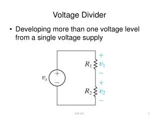
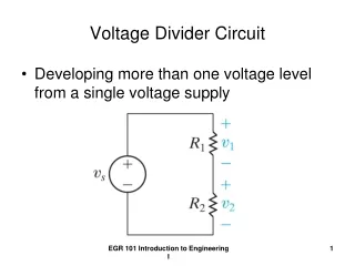
Voltage-divider bias configuration ENGI 242/ELEC 222
Voltage Divider Input Circuit Approximate Analysis This method is valid only ifR2 .1 RE Under these conditions RE does not significantly load R2 and it may be ignored: IB << I1and I2 and I1 I2Therefore: • We may apply KVL to the input, which gives us: • -VB + VBE + IE RE = 0 • Solving for IE we get: ENGI 242/ELEC 222
Input Circuit Exact Analysis This method is always valid must be used when R2> .1 RE Perform Thevenin’s Theorem Open the base lead of the transistor, and the Voltage Divider bias circuit is: Calculate RTH We may apply KVL to the input, which gives us: -VTH + IB RTH + VBE + IE RE = 0 Since IE = ( + 1) IB ENGI 242/ELEC 222
Redrawing the input circuit for the network ENGI 242/ELEC 222
Determining VTH ENGI 242/ELEC 222
Determining RTH ENGI 242/ELEC 222
The Thévenin Equivalent Circuit Note that VE = VB – VBE and IE = ( + 1)IB ENGI 242/ELEC 222
Input Circuit Exact Analysis We may apply KVL to the input, which gives us: -VTH + IB RTH + VBE + IE RE = 0 Since IE = ( + 1) IB ENGI 242/ELEC 222
Collector-Emitter Loop ENGI 242/ELEC 222
Collector-Emitter (Output) Loop Applying Kirchoff’s voltage law: - VCC + IC RC + VCE + IE RE = 0 Assuming that IE IC and solving for VCE: Solve for VE: VE = IE RE Solve for VC: VC = VCC - IC RC or VC = VCE + IE RE Solve for VB: VB = VCC - IB RB or VB = VBE + IE RE ENGI 242/ELEC 222
Voltage Divider Bias Example 1 VCC = 22V R1 = 39k R2 = 3.9k RC = 10k RE = 1.5k = 140 ENGI 242/ELEC 222
Voltage Divider Bias Example 2 VCC = 18V R1 = 39k R2 = 8.2k RC = 3.3k RE = 1k = 120 ENGI 242/ELEC 222
Voltage Divider Bias Example 3 VCC = 16V R1 = 62k R2 = 9.1k RC = 3.9k RE = .68k = 80 ENGI 242/ELEC 222
Design of CE Amplifier with Voltage Divider Bias • Select a value for VCC • Determine the value of from spec sheet or family of curves • Select a value for ICQ • Let VCE = ½ VCC (typical operation, 0.4 VCC≤ VC≤ 0.6 VCC) • Let VE = 0.1 VCC(for good operation, 0.1 VCC≤ VE≤ 0.2 VCC) • Calculate RE and RC • Let R2≤ 0.1 RE (for this calculation, use low value for ) • Calculate R1 ENGI 242/ELEC 222
CE Amplifier Design • Design a Common Emitter Amplifier with Voltage Divider Bias for the following parameters: VCC = 24V IC = 5mA VE = .1VCC VC = .55VCC = 135 ENGI 242/ELEC 222
CE Amplifier Design ENGI 242/ELEC 222
CE Amplifier Design Voltage Divider Bias ENGI 242/ELEC 222
Collector Feedback Bias ENGI 242 ELEC 222
BJT Biasing 4 For the Collector Feedback Bias Configuration: • Draw Equivalent Input circuit • DrawEquivalent Output circuit • Write necessary KVL and KCL Equations • Determine the Quiescent Operating Point • Graphical Solution using Loadlines • Computational Analysis • Design and test design using a computer simulation ENGI 242/ELEC 222
DC Bias with Collector (Voltage) Feedback Another way to improve the stability of a bias circuit is to add a feedback path from collector to base In this bias circuit the Q-point is only slightly dependent on the transistor ENGI 242/ELEC 222
Base – Emitter Loop Solve for IB Applying Kirchoff’s voltage law: -VCC + ICRC + IBRB + VBE + IERE = 0 Note: IC = IE = IC + IB Since IE = ( + 1) IB then: -VCC + ( + 1)IB RC + IBRB + VBE ( + 1)IBRE = 0 Simplifying and solving for IB: ENGI 242/ELEC 222
Base – Emitter Loop Solve for IE Applying Kirchoff’s voltage law: -VCC + IERC + IBRB + VBE + IERE = 0 Since IE = ( + 1) IB then: Simplifying and solving for IE: ENGI 242/ELEC 222
Collector Emitter Loop Applying Kirchoff’s voltage law: IE RE + VCE + ICRC – VCC = 0 Since IC= IE and IE = ( + 1) IB: IE(RC + RE) + VCE – VCC =0 Solving for VCE: VCE = VCC – IE (RE + RC) ENGI 242/ELEC 222
Network Example ENGI 242/ELEC 222
Network Example ENGI 242/ELEC 222
Collector feedback with RE = 0 ENGI 242/ELEC 222
Design of CE Amplifier with Collector Feedback Bias • Select a value for VCC • Determine the value of from spec sheet or family of curves • Select a value for IEQ • Let VCE = ½ VCC (typical operation, 0.4 VCC≤ VC≤ 0.6 VCC) • Let VE = 0.1 VCC(for good operation, 0.1 VCC≤ VE≤ 0.2 VCC) • Calculate RE, RC and RB ENGI 242/ELEC 222
Voltage Divider Bias with Dual Power Supply ENGI 242/ELEC 222
Voltage Divider Bias with Dual Power Supply Input Circuit Find VTH and RTH ENGI 242/ELEC 222
Voltage Divider Bias with Dual Power Supply Output Circuit ENGI 242/ELEC 222
Voltage Divider Bias with Dual Power Supply ENGI 242/ELEC 222
PSpice Bias Point Simulation ENGI 242/ELEC 222
PSpice Simulation for DC Bias ENGI 242/ELEC 222
PSpice Simulation for DC Sweep ENGI 242/ELEC 222
PSpice Simulation for DC Sweep The response of VC demonstrates rises rapidly towards the Q Point and then increases gradually towards a maximum value The response of VCE demonstrates that it reaches a peak value near the Q point and then decreases ENGI 242/ELEC 222
PSpice Simulation for AC Sweep ENGI 242/ELEC 222
PSpice Simulation for AC Sweep ENGI 242/ELEC 222