Download

1 / 69
860 likes | 1.34k Views
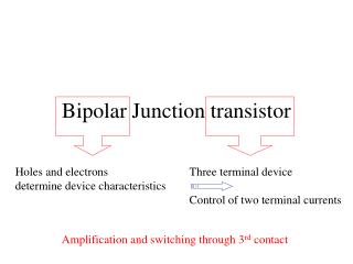
Bipolar Junction Transistor Basics. C. BJTs. B. E. The BJT – Bipolar Junction Transistor. Note: Normally Emitter layer is heavily doped, Base layer is lightly doped and Collector layer has Moderate doping. The Two Types of BJT Transistors :. npn. pnp. n. p. n. p. n. p. E. C. E.

E N D
Bipolar Junction Transistor Basics C BJTs B E
The BJT – Bipolar Junction Transistor Note: Normally Emitter layer is heavily doped, Base layer is lightly doped and Collector layer has Moderate doping. The Two Types of BJT Transistors: npn pnp n p n p n p E C E C C C Cross Section Cross Section B B B B Schematic Symbol Schematic Symbol E E • Collector doping is usually ~ 109 • Base doping is slightly higher ~ 1010 – 1011 • Emitter doping is much higher ~ 1017
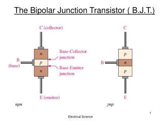
BJT Relationships - Equations IE IC IE IC - VCE + + VEC - E C E C - - + + VBE VBC IB VEB VCB IB - - + + B B n p n IE = IB + IC VCE = -VBC + VBE p n p IE = IB + IC VEC = VEB - VCB Note: The equations seen above are for the transistor, not the circuit.
n I co - Inc + VCB - p- - Electrons + Holes + Ipe Ine n+ VBE - Bulk-recombination Current Figure : Current flow (components) for an n-p-n BJT in the active region. NOTE: Most of the current is due to electrons moving from the emitter through base to the collector. Base current consists of holes crossing from the base into the emitter and of holes that recombine with electrons in the base.
Physical Structure • Consists of 3 alternating layers of n- and p-type semiconductor called emitter (E), base (B) and collector (C). • Majority of current enters collector, crosses base region and exits through emitter. A small current also enters base terminal, crosses base-emitter junction and exits through emitter. • Carrier transport in the active base region directly beneath the heavily doped (n+) emitter dominates i-v characteristics of BJT.
Ic C - - - - - - - - - - - - - - - - - n Recombination VCB + _ • Electrons • + Holes B - - - - - - + - - + - - p + + IB - VBE - _ • - - - - - - • - - • - - - - - - • - - - • - • - - - - - - - - n E IE
For CB Transistor IE= Ine+ Ipe Ic= Inc- Ico And Ic= - αIE + ICo CB Current Gain, α ═ (Ic- Ico) . (IE- 0) For CE Trans., IC = βIb + (1+β) Ico where β═α , 1- α is CE Gain Bulk-recombination current ICO Inc Ipe Ine Figure: An npn transistor with variable biasing sources (common-emitter configuration).
Common-Emitter Circuit Diagram Collector-Current Curves VCE IC IC + _ Active Region VCC IB IB VCE Saturation Region Cutoff Region IB = 0
BJT’s have three regions of operation: 1) Active - BJT acts like an amplifier (most common use) 2) Saturation - BJT acts like a short circuit 3) Cutoff - BJT acts like an open circuit BJT is used as a switch by switching between these two regions. When analyzing a DC BJT circuit, the BJT is replaced by one of the DC circuit models shown below. DC Models for a BJT:
DC and DC = Common-emitter current gain = Common-base current gain = IC = IC IB IE The relationships between the two parameters are: = = + 1 1 - Note: and are sometimes referred to as dc and dc because the relationships being dealt with in the BJT are DC.
Output characteristics: npn BJT (typical) Note: The PE review text sometimes uses dc instead of dc. They are related as follows: • Find the approximate values of bdc and adc from the graph. Input characteristics: npn BJT (typical) The input characteristics look like the characteristics of a forward-biased diode. Note that VBE varies only slightly, so we often ignore these characteristics and assume: Common approximation: VBE = Vo = 0.65 to 0.7V Note: Two key specifications for the BJT are Bdc and Vo (or assume Vo is about 0.7 V)
Figure: Common-emitter characteristics displaying exaggerated secondary effects.
Figure: Common-emitter characteristics displaying exaggerated secondary effects.
Various Regions (Modes) of Operation of BJT Active: • Most important mode of operation • Central to amplifier operation • The region where current curves are practically flat Saturation: • Barrier potential of the junctions cancel each other out causing a virtual short (behaves as on state Switch) Cutoff: • Current reduced to zero • Ideal transistor behaves like an open switch * Note: There is also a mode of operation called inverse active mode, but it is rarely used.
BJT Trans-conductance Curve For Typical NPN Transistor 1 Collector Current: IC = IES eVBE/VT Transconductance: (slope of the curve) gm = IC/ VBE IES = The reverse saturation current of the B-E Junction. VT = kT/q = 26 mV (@ T=300oK) = the emission coefficient and is usually ~1 IC 8 mA 6 mA 4 mA 2 mA VBE 0.7 V
Three Possible Configurations of BJT Biasing the transistor refers to applying voltages to the transistor to achieve certain operating conditions. 1. Common-Base Configuration (CB) : input = VEB & IE output = VCB & IC 2. Common-Emitter Configuration (CE): input = VBE & IB output= VCE & IC 3. Common-Collector Configuration (CC) :input = VBC & IB (Also known as Emitter follower) output = VEC & IE
Common-Base BJT Configuration VCE IC IE C E VCB VBE IB + _ + _ B VCB VBE Circuit Diagram: NPN Transistor The Table Below lists assumptions that can be made for the attributes of the common-base BJT circuit in the different regions of operation. Given for a Silicon NPN transistor.
Common-Base (CB) Characteristics Although the Common-Base configuration is not the most common configuration, it is often helpful in the understanding operation of BJT Vc- Ic (output) Characteristic Curves IC mA Breakdown Reg. 6 Active Region IE 4 IE=2mA Saturation Region 2 IE=1mA Cutoff IE = 0 VCB 0.8V 2V 4V 6V 8V
Common-Collector BJT Characteristics Emitter-Current Curves IE The Common-Collector biasing circuit is basically equivalent to the common-emitter biased circuit except instead of looking at IC as a function of VCE and IB we are looking at IE. Also, since ~ 1, and = IC/IE that means IC~IE Active Region IB VCE Saturation Region Cutoff Region IB = 0
n p n Transistor: Forward Active Mode Currents Base current is given by IC= IB= is forward common-emitter current gain Emitter current is given by VBE IE= Forward Collector current is Ico is reverse saturation current is forward common- base current gain In this forward active operation region, VT = kT/q =25 mV at room temperature
Various Biasing Circuits used for BJT • Fixed Bias Circuit • Collector to Base Bias Circuit • Potential Divider Bias Circuit
The Thermal Stability of Operating Point SIco The Thermal Stability Factor : SIco SIco = ∂Ic ∂Ico This equation signifies that Ic Changes SIco times as fast as Ico Differentiating the equation of Collector Current IC & rearranging the terms we can write SIco ═ 1+β 1- β (∂Ib/∂IC) It may be noted that Lower is the value of SIco better is the stability Vbe,β
The Fixed Bias Circuit The Thermal Stability Factor : SIco SIco = ∂Ic ∂Ico General Equation of SIco Comes out to be SIco ═ 1 + β 1- β (∂Ib/∂IC) Vbe, β RC Rb RC Applying KVL through Base Circuit we can write, Ib Rb+ Vbe= Vcc Diff w. r. t. IC, we get (∂Ib / ∂Ic) = 0 SIco= (1+β) is very large Indicating high un-stability Ib
The Collector to Base Bias Circuit The General Equation for Thermal Stability Factor, SIco = ∂Ic ∂Ico Comes out to be SIco ═ 1 + β 1- β (∂Ib/∂IC) Vbe, β Ic Applying KVL through base circuit we can write (Ib+ IC) RC + Ib Rb+ Vbe= Vcc Diff. w. r. t. IC we get (∂Ib / ∂Ic) = - RC / (Rb + RC) Therefore, SIco ═ (1+ β) 1+ [βRC/(RC+ Rb)] Which is less than (1+β), signifying better thermal stability Ib + VBE IE -
The General Equation for Thermal Stability Factor, SIco ═ 1 + β 1- β (∂Ib/∂IC) The Potential Devider Bias Circuit IC Applying KVL through input base circuit we can write IbRTh + IE RE+ Vbe= VTh Therefore, IbRTh + (IC+ Ib) RE+ VBE= VTh Diff. w. r. t. IC & rearranging we get (∂Ib / ∂Ic) = - RE / (RTh + RE) Therefore, This shows that SIco is inversely proportional to RE and It is less than (1+β), signifying better thermal stability Ib IC Thevenin Equivalent Ckt IC Ib Rth= R1*R2 &Vth = Vcc R2 R1+R2 R1+R2 Self-bias Resistor Thevenins Equivalent Voltage
A Practical C E Amplifier Circuit Input Signal Source
BJT Amplifier (continued) If changes in operating currents and voltages are small enough, then IC and VCE waveforms are undistorted replicas of the input signal. A small voltage change at the base causes a large voltage change at the collector. The voltage gain is given by: The minus sign indicates a 1800 phase shift between input and output signals. An 8 mV peak change in vBE gives a 5 mA change in iB and a 0.5 mA change in iC. The 0.5 mA change in iC gives a 1.65 V change in vCE .
A Practical BJT Amplifier using Coupling and Bypass Capacitors In a practical amplifier design, C1 and C3 are large coupling capacitors or dc blocking capacitors, their reactance (XC = |ZC| = 1/wC) at signal frequency is negligible. They are effective open circuits for the circuit when DC bias is considered. C2 is a bypass capacitor. It provides a low impedance path for ac current from emitter to ground. It effectively removes RE (required for good Q-point stability) from the circuit when ac signals are considered. • AC coupling through capacitors is used to inject an ac input signal and extract the ac output signal without disturbing the DC Q-point • Capacitors provide negligible impedance at frequencies of interest and provide open circuits at dc.
D C Equivalent for the BJT Amplifier (Step1) • All capacitors in the original amplifier circuit are replaced by open circuits, disconnecting vI, RI, and R3 from the circuit and leaving RE intact. The the transistor Q will be replaced by its DC model. DC Equivalent Circuit
A C Equivalent for the BJT Amplifier (Step 2) Ro R1IIR2=RB Rin • Coupling capacitor CC and Emitter bypass capacitor CE are replaced by short circuits. • DC voltage supply is replaced with short circuits, which in this case is connected to ground.
A C Equivalent for the BJT Amplifier (continued) All externally connected capacitors are assumed as short circuited elements for ac signal • By combining parallel resistors into equivalent RBand R, the equivalent AC circuit above is constructed. Here, the transistor will be replaced by its equivalent small-signal AC model (to be developed).
1)Determine DC operating point and calculate small signal parameters 2) Draw the AC equivalent circuit of Amp. • DC Voltage sources are shorted to ground • DC Current sources are open circuited • Large capacitors are short circuits • Large inductors are open circuits 3)Use a Thevenin circuit (sometimes a Norton) where necessary. Ideally the base should be a single resistor + a single source. Do not confuse this with the DC Thevenin you did in step 1. 4) Replace transistor with small signal model 5) Simplify the circuit as much as necessary. Steps to Analyze a Transistor Amplifier 6)Calculate the small signal parameters and gain etc. A C Analysis of CE Amplifier Step 1 Step 2 Step 3 Step 4 Step 5 π-model used
Hybrid-Pi Model for the BJT Transconductance: • The hybrid-pi small-signal model is the intrinsic low-frequency representation of the BJT. • The small-signal parameters are controlled by the Q-point and are independent of the geometry of the BJT. Input resistance: Rin Output resistance: Where, VA is Early Voltage (VA=100V for npn)
Hybrid Parameter Model Ii Io Linear Two port Device Vo Vi
h-Parameters h11 = hi = Input Resistanceh12 = hr = Reverse Transfer Voltage Ratioh21 = hf = Forward Transfer Current Ratioh22 = ho = Output Admittance
Three Small signal Models of CE Transistor The Mid-frequency small-signal models
BJT Mid-frequency Analysis using the hybrid-p model: A common emitter (CE) amplifier • The mid-frequency circuit is drawn as follows: • the coupling capacitors (Ci and Co) and the • bypass capacitor (CE) are short circuits • short the DC supply voltage (superposition) • replace the BJT with the hybrid-p model • The resulting mid-frequency circuit is shown below. An a c Equivalent Circuit ro
Details of Small-Signal Analysis for Gain Av (Using Π-model) Rs Rs From input circuit
C-E Amplifier Input Resistance • The input resistance, the total resistance looking into the amplifier at coupling capacitor C1, represents the total resistance presented to the AC source.
C-E Amplifier Output Resistance • The output resistance is the total equivalent resistance looking into the output of the amplifier at coupling capacitor C3. The input source is set to 0 and a test source is applied at the output. But vbe=0. since ro is usually >> RC.
High-Frequency Response – BJT Amplifiers Capacitances that will affect the high-frequency response: • Cbe, Cbc, Cce – internal capacitances • Cwi, Cwo – wiring capacitances • CS, CC – coupling capacitors • CE – bypass capacitor
Frequency Response of Amplifiers The voltage gain of an amplifier is typically flat over the mid-frequency range, but drops drastically for low or high frequencies. A typical frequency response is shown below. • For a CE BJT: (shown on lower right) • low-frequency drop-off is due to CE, Ci and Co • high-frequency drop-off is due to device capacitances Cp and Cm (combined to form Ctotal) • Each capacitor forms a break point (simple pole or zero) with a break frequency of the form f=1/(2pREqC), where REq is the resistance seen by the capacitor • CE usually yields the highest low-frequency break • which establishes fLow.
Amplifier Power Dissipation • Static power dissipation in amplifiers is determined from their DC equivalent circuits. Total power dissipated in C-B and E-B junctions is: where Total power supplied is: The difference is the power dissipated by the bias resistors.
An Emitter Follower (CC) Amplifier Figure Emitter follower. Very high input Resistance Very low out put Resistance Unity Voltage gain with no phase shift High current gain Can be used for impedance matching or a circuit for providing electrical isolation
Capacitor Selection for the CE Amplifier The key objective in design is to make the capacitive reactance much smaller at the operating frequency f than the associated resistance that must be coupled or bypassed.