Download
1 / 33
380 likes | 782 Views
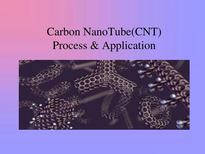
Carbon NanoTube(CNT) Process & Application. OUTLINE. Introduction History Structure Synthesis Properties Application Challenges References. What is CNT?. CNT is a tubular form of carbon with diameter as small as 1nm. Length: few nm to microns. CNT is configurationally equivalent

E N D
OUTLINE Introduction History Structure Synthesis Properties Application Challenges References
What is CNT? CNT is a tubular form of carbon with diameter as small as 1nm. Length: few nm to microns. CNT is configurationally equivalent to a two dimensional graphene sheet rolled into a tube. Can have caps at the ends making them look like pills
What CNT Really look like! Clumps, ropes, Bundles, mats Very high tendency to stick together
History In 1970s, Morinobu Endo prepared the first carbon filament of nanometer dimensions Richard E. Smalley (Nobel Prize winning in 1996) discovered the buckyball (C60) and other fullerenes (1985) In 1991, Sumio Iijima had been using TEM To analyze new type of finite carbon structure, that is composed of needle-like tubes
Structure • The structure of CNT can be represented based on 2D graphene lattice. • Properties depending only on tube diameter and chiral angle. • For a random chirality distribution,1/3 of the nanotubes are metallic
Cont What is so unique about CNT is due to the different electrical and thermal conductivities they exhibit when their hexagonal structures are orientated differently. For instance, armchair, chiral and zig-zag structure allow the CNT to act like metal, semiconductor and insulator, respectively. The difference in orientation can be determined by a method of measurement termed chiral vector . Chiral Vector: Ch = n â1 + m â2, Chiral Angle
Armchair: n=m = 30 Chiral: n!=m 0 < < 30 Zig zag: m=0 = 0 Where n and m are the number of unit vector along two directions in the honeycomb crystal lattice of graphene. Cont..
Cont… Carbon nanotubes can be metallic or semiconductor depending on their chirality Chiral Vector C is defined as the vector from one open end of the tube to the other after it is rolled If (n-m) is divisible by 3, the tube is metallic If (n-m) is not divisible by 3, the tube is semiconducting.
Why do Carbon Nanotubes form? Carbon Graphite (Ambient conditions) sp2 hybridization: planar Diamond (High temperature and pressure) sp3 hybridization: cubic Nanotube/Fullerene (certain growth conditions) sp2 + sp3 character: cylindrical Finite size of graphene layer has dangling bonds. These dangling bonds correspond to high energy states. Eliminates dangling bonds Nanotube formation + Total Energy Increases Strain Energy decreases
Types of CNTs Single Wall CNT (SWCNT) Consist of just one layer of carbon average diameter 1.2 nm Multiple Wall CNT (MWCNT) Consist of 2 or more layers of carbon average diameter 20 nm (Can be metallic or semiconducting depending on their geometry)
Synthesis of CNT’s Evaporation of solid carbon in arc discharge Laser ablation Catalytic chemical vapor deposition of carbon containing gases
Arc Discharge • Traditional method • carried out in a medium of a Nobel Gas such as Helium or Argon. • requires complex vacuum equipments. • Such methods are, not only expensive but rather, time consuming too. • only MWNT and ropes
Cont.. Two carbon electrodes are kept with a gap in between. When high current, about 80 A is passed through the electrodes where gap is filled with helium under 300 torr. Cylindrical deposit then grows at about 2 to 3 mm per minute. This cathode deposit contains two portions: the inside is a black fragile core and the outside a hard shell.
Laser Abaltion • A well mixed acetylene-air mixture is burned inside a tube furnace • A laser is used to vaporize a metal target (either Fe or Ni) • The post-flame exhaust gas is mixed with the metallic vapor and allowed to cool • During cooling, carbon nanotubes are formed • Spongy black deposit • Diameters, chiralities, metallic or semiconductor all uncontrolled
Chemical vapor Depostion(CVD) Single SWNT for the 1st time. Aligned nanotubes Large scale possible Relatively cheap Diameters, chiralities, metallic or semiconductor all uncontrolled
Cont… In CVD, a substrate is prepared with a layer of metal catalyst particles, most commonly nickel, cobalt, iron, or a combination. The metal nanoparticles can also be produced by other ways, including reduction of oxides or oxides solid solutions. The diameters of the nanotubes that are to be grown are related to the size of the metal particles. The substrate is heated to approximately 700°C. To initiate the growth of nanotubes, two gases are bled into the reactor: a process gas (such as ammonia, nitrogen, hydrogen, etc.) and a carbon-containing gas (such as acetylene, ethylene, ethanol, methane, etc.). Nanotubes grow at the sites of the metal catalyst; the carbon-containing gas is broken apart at the surface of the catalyst particle, and the carbon is transported to the edges of the particle, where it forms the nanotubes
Properties Electrical conductivity six orders of magnitude higher than copper Can be metallic or semiconducting depending on chirality - ‘tunable’ bandgap - electronic properties can be tailored through application of external magnetic field, application of mechanical deformation… Very high current carrying capacity Excellent field emitter; high aspect ratio and small tip radius of curvature are ideal for field emission
The strongest and most flexible molecular material because of C-C covalent bonding and seamless hexagonal network architecture Young’s modulus of over 1 TPa vs 70 GPa for Aluminum strength to weight ratio 500 time > for Al; similar improvements over steel and titanium; one order of magnitude improvement over graphite/epoxy Maximum strain ~10% much higher than any material Thermal conductivity ~ 3000 W/mK in the axial direction with small values in the radial direction Cont….
Electronics • quantum wire interconnects • Diodes and transistors for computing • Capacitors • Data Storage • Field emitters for instrumentation • Flat panel displays
Carbon Nanotube FET • First CNT-FET fabricated in 1998 CNT can be used as the conducting channel of a MOSFET. • These new devices are very similar to the CMOS FETs. • All CNFETs are pFETs by nature. • nFETs can be made through • Annealing • Doping • Very low current and power consumption • Although tubes are 3nm thick CNFETs are still the size of the contacts, about 20nm.
Interconnect Today chips have become “all wires” Electro-migration failure
CNT interconnect • High current density • Low resistance (6.2k ohm) • Ballistic behavior
Cont…. SENSORS,NEMS,BIO • CNT based microscopy: AFM, STM…CNT tip is robust ,offers amazing resolution. • Nanotube sensors: force, pressure, chemical… • Biosensors • Molecular gears, motors, actuators • Batteries, Fuel Cells: H2, Li storage • Biomedical - Lab on a chip - Drug delivery - DNA sequencing ScanningProbe Simulated Mars dust
Challenges • Selective placement of CNTs • Control of diameter, chirality • Doping, contacts • Novel architectures (not CMOS based!) • Large scale production • Development of inexpensive manufacturing processes
Stanford Model Two set of files: CNFET.lib - CNFET Models. PARAMETERS.lib - Global parameters for the model. To instantiate the devices in the model, the library must be included at the beginning of the SPICE file. .lib ‘CNFET.lib’ CNFET
CNT Model The model is implemented hierarchically in three levels: CNFET_L1: Level 1, models the intrinsic behavior of MOSFET- like CNFET. CNFET_L2: Level 2, models the device non-idealities (capacitance and resistance of doped S/D CNT region). CNFET_L3: Level 3, models the interface between the CNFET device and CNFET circuits.
Metal Gate CNT Intrinsic CNT channel Substrate Substrate CNTFET_L1 CNFET_L2 CNT’s G/S/D Metal Gate G/S/D Substrate CNFET_L3
References • You can see animations of virtual nanotubes by following these links: http://www.photon.t.u-tokyo.ac.jp/~maruyama/nanotube.html http://www.pa.msu.edu/cmp/csc/simindex.html • You can create your own virtual SWNT at: http://jcrystal.com/steffenweber/JAVA/jnano/jnano.html “Chemical Vapor Deposition.” http://www.sandia.gov/1100/CVDwww/cvdinfo.htm “Physical Properties of Carbon Nanotubes.” http://www.pa.msu.edu/cmp/csc/ntproperties/