Download
1 / 40
400 likes | 498 Views
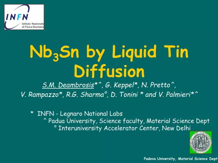
Nb 3 Sn by Liquid Tin Diffusion. S.M. Deambrosis *^, G. Keppel*, N. Pretto^, V. Rampazzo*, R.G. Sharma°, D. Tonini * and V. Palmieri*^. * INFN - Legnaro National Labs ^ Padua University, Science faculty, Material Science Dept ° Interuniversity Accelerator Center, New Delhi.

E N D
Nb3Sn by Liquid TinDiffusion S.M. Deambrosis*^, G. Keppel*, N. Pretto^, V. Rampazzo*, R.G. Sharma°, D. Tonini *and V. Palmieri*^ * INFN - Legnaro National Labs ^ Padua University, Science faculty, Material Science Dept ° Interuniversity Accelerator Center, New Delhi Padova University, Material Science Dept
1) Theory Vapor Sndiffusion 2) Literature review 3) Technique choice reasons Liquid Sn diffusion Nb3Sn by liquid Sn diffusion Used system 4) Method “1 Step” process 5) Work in progress “2 Steps” process “Hybrid” process 6) Conclusions
RBCS If T < Tc / 2 Empirically, Rres is found to be dependent on rn too. A metallic behaviour in the normal state is mandatory For low rf losses, a high TC value is not sufficient Theory
Nomogram At T = 4.2 K, f = 500 MHz, s = 4, RBCS depends on Δ and ρn RBCS Ideal R BCS ~ 1 nΩ ~ 10 μΩcm Theory
Literature review Many papers of different authors with different aims: • Nb3Sn by CVD and PVD techniques to compare bulk and film properties • Nb3Sn by bronze process for high field Superconducting Magnets • Nb3Sn RF application: Wuppertal Literature
Wuppertal: Nb3Sn cavity (1.5 GHz) obtained trough Sn vapour phase diffusion (’90s) Literature
Vapor Sn Diffusion Heating system Accelerating structure Sn source Sn source heater Pumping system Laboratory Procedure • Cavity manufactoring • Formation of nucleation centers of Nb3Sn (Nb Surface Anodization + SnCl2 Treatment) • Nb3Sn film growth in a Sn atmosphere (T = 1050-1250°C, t = dozens of h, p(Sn) ~ 10-3mbar) • Cool down and unwanted phases Chemical removal (anodizaton + HF 48%) Technique Choice Reasons
Liquid solute diffusion technique Technique Choice Reasons
Liquid Sn Diffusion? Bulk Nb substrate dipping in a liquid Tin bath Sample Annealing • No nucleation sites on Nb are required • Fast growth of Nb3Sn layer • Deasirable uniform thickness Technique Choice Reasons
Used System Method: used system
Nb3Sn: Phase Diagram Nb3Sn 930°C <Tc phases Method: used system
To Summarise ●Liquid solute diffusion technique choice ●Working T > 930 °C
“1 Step” Process Laboratory Procedure • Bulk Nb Substrate chemical cleaning (10 min in a 1:1:2 solution) • Substarte fixing to feedtrough, vacuum and T reaching (1 day) • Substrate thermalization (30 min - 1 h) • Dipping (few min - 2 h) • Annealing above the Sn bath without opening the chamber(some h) • Residual Sn Chemical removal trials Method: “1 step” process
Nb3Sn photo Residual Sn Sn drop Method: “1 step” process
SEM Image Process T = 1000°C Dipping t = 120’ Annealing t = 14h Post annealing: 5h at 500°C Nb3Sn Nb Method: “1 step” process
XRD spectrum Process T = 1000°C, Dipping t = 30’, Annealing t = 10h Method: “1 step” process
EMPA Analysis Method: “1 step” process
A Superconductive Transition Curve Nb3Sn n°16: 1000°C; 120’+14h+post annealing 500°Cx5h Method: “1 step” process
6 GHz Cavities • Spinning Technique 2. Surface Treatments • Mechanical polishing • Chemical polishing • Nb3Sn film obtainment 3. Q Factor Measurement Method: “1 step” process
Nb3Sn film obtainment Film production: T = 1025°C tdipping = 15 min, tannealing = 15 h Chemical treatment: HCl 37%, t = 10 min, T = 85°C Method: “1 step” process
Q Factor Measurement Nb3Sn Method: “1 step” process
A Nb3Sn 6 GHz Cavity Method: “1 step” process
To Summarise Nb3Sn with good superconductive properties + Tc = 16,9 K DTc= 0,2 K - Residual Sn traces on the sample surface - Sn rich Phases Presence Method: “1 step” process
“2 Steps” Process Laboratory Procedure • Bulk Nb Substrate chemical cleaning (10 min in a 1:1:2 solution) • Substarte fixing to the feedtrough, vacuum and T reaching (1 day) • Substrate thermalization (30 min - 1 h) • Dipping (few min - 2 h) • System opening to remove Sn bath, vacuum and T reaching (1 day) • Sample annealing without Sn vapor (some h) • Growth film chemical treatment Method: “2 steps” process
Nb3Sn photo Method: “2 steps” process
SEM Images Proc T = 1025°C, Dipp t = 15’, Ann t = 15h Proc T = 1025°C, Dipp t = 5’, Ann t = 20h Method: “2 steps” process
XRD spectra Proc T = 1025°C, Dipp t = 5’, Ann t = 20h Proc T = 1025°C, Dipp t = 5’, Ann t = 10h Method: “2 steps” process
A Superconductive Transition Curve Proc T = 1025°C, Dipp t = 5’, Ann t = 20h Tc (Nb3Sn) = 14,9 K DTc (Nb3Sn) = 0,43 K Method: “2 steps” process
Growth film chemical treatment (HCl) Method: “2 steps” process
Tc and DTc vs THCl Method: “2 steps” process
To Summarise + No Residual Sn traces on the sample surface Worst Nb3Sn film superconductive properties - Tc = 15,2 K, DTc = 0,5 K - Sn rich Phases Presence HCl chemical treatment deteriorates the growth film - Method: “2 steps” process
“Hybrid” Process Laboratory Procedure • Bulk Nb Substrate chemical cleaning (10 min in a 1:1:2 solution) • Substarte fixing to the feedtrough, vacuum and T reaching (1 day) • Substrate thermalization (30 min - 1 h) • Dipping (few min - 2 h) • Sample annealing with Sn vapor (some h) • System opening to remove Sn bath, vacuum and T reaching (1 day) • Sample annealing without Sn vapor (some h) Method: “Hybrid” process
Nb3Sn photo Method: “Hybrid” process
XRD spectrum Proc T = 975°C, Dipp t = 30’, Ann (Sn) t = 2h, Ann t = 5h Method: “Hybrid” process
A Superconductive Transition Curve Proc T = 975°C, Dipp t = 30’, Ann (Sn) t = 2h, Ann t = 5h Tc (Nb3Sn) = 16,6 K DTc (Nb3Sn) = 0,28 K Method: “Hybrid” process
To Summarise + No Residual Sn traces on the sample surface Good Nb3Sn film superconductive properties + Tc = 16,5 K, DTc = 0,3 K + No Sn rich Phases Method: “Hybrid” process
Work in progress • Two furnaces system to avoid air contamination of the superconducting thin film while opening the vacuum system • Use of the best results to coat 6 GHz Nb cavities for a Nb3Sn RF properties sistematic testing • Use of a different experimental method to prepare Nb3Sn: • multilayer obtained altermatively depositing Nb and Sn
Conclusions • Liquid solute diffusion technique (working T > 930 °C) • Three different processes: • “1 step” • “2 steps” • “Hybrid” • trying to optimize T and t • Finally: • ◊ Good superconducting properties • ◊ No Sn • ◊ No Sn rich Phases