Download
1 / 1
10 likes | 136 Views
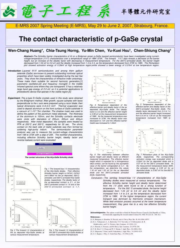
半導體元件 研究室. E-MRS 2007 Spring Meeting (E-MRS), May 29 to June 2, 2007, Strabourg, France. The contact characteristic of p-GaSe crystal. Wen-Chang Huang*, Chia-Tsung Horng, Yu-Min Chen, Yu-Kuei Hsu 1 , Chen-Shiung Chang 1.

E N D
半導體元件研究室 E-MRS 2007 Spring Meeting (E-MRS), May 29 to June 2, 2007, Strabourg, France. The contact characteristic of p-GaSe crystal Wen-Chang Huang*, Chia-Tsung Horng, Yu-Min Chen, Yu-Kuei Hsu1, Chen-Shiung Chang1 Abstract--The Schottky barrier characteristics of Al on a Bridgman grown p-GaSe layered semiconductor have been investigated using current-voltage-temperature (I-V-T) characteristics over a temperature range of 198K~373K. The forward I-V-T data reveals a decrease at the barrier height, but an increase at the ideality factor with decreasing in measurement temperature. For the 300C-annealed diode, the barrier height decreased from 1.04 eV to 0.6 eV and the ideality increased from 1.4 to 2.4, as the temperature decreased from 373K to 198K. The Richardson plot showed activation energy of 0.26eV at high temperature region,while showed a lower energy of 0.07eV at low temperature region. Introduction--Layered III-VI semiconductors and among them gallium selenide (GaSe) are known to present outstanding nonlinear optical properties which have been widely investigated during the last few years. They show the characteristics of refractive index anisotropy. These make them suitable for second harmonic generation,[1] parametric oscillation,[2] and frequency mixing[3] in the middle infrared spectral zone where they are transparent. It has a relatively large band gap energy of 2.0 eV, so it is potential applications to photoelectric device that operate in the visible region.[5] Experiment--The p-type Er:GaSe crystals used in this study were obtained by the Bridgmann method. After growth, square samples with faces perpendicular to the c axis were prepared using a razor blade; their typical dimensions were 440.3 mm3. Thermal evaporator was used to deposit aluminum on the front surface of GaSe substrate in a vacuum of 110-4 Torr chamber. The shadow mask was used to define the pattern of the aluminum metal electrode. The thickness of the aluminum is 100nm, and the Schottky contacts electrode were circle with diameters of 200m, 300m and 400m respectively. After metal deposition, the samples were treated by RTA at 200C and 300C, respectively for 30 sec. The ohmic contact on the back side of GaSe substrate was then formed by soldering high-purity indium. The semiconductor parameter analyzer was use to measure the current-voltage characteristics from 198 to 373K with a step of 25K. The rectified characteristics, including effective Schottky barrier height, ideality factor and reverse leakage current were evaluated. Fig. 5 Temperature dependent of the effective barrier and ideality factor of the 300C-annealed Al/p-GaSe diode. The ideality factor decreased from 2.4 to 1.4 and the effective barrier height increased from 0.4 eV to 1.04 eV as the measured temperature increased from 198K to 373K. Fig. 4 Temperature dependent of the effective barrier and ideality factor of the as deposited Al/p-GaSe diode. The ideality factor is 3.3 and the effective barrier height is 0.59 eV at the measurement temperature of 198K. As the measured temperature was increased to 373K, the ideality factor was decreased to 1.81 and the effective barrier height was increased to 1.03eV. Fig. 6 The relationship between effective barrier height and ideality factor at different measured temperature. The effective barrier height which is expected for a homogeneous ideal contact, can be found by the asymptotic value of the barrier extrapolated at n=1. By the extrapolation, we determine the values 1.18 eV and 1.22 eV for the as deposited diode and the 300C-annealed annealed diode, respectively. Fig. 7 Richardson plots of the Al/p-GaSe diode, respectively. The corresponding activation energy was evaluated which is 0.32eV for the as deposited diode and is 0.27 eV for the 300C annealed diode. As the measurement temperature below 300K, the activation energy is 0.05 eV for as deposited diode, is 0.067 eV for thev300C-annealed diode. The contact structure of the Al/p-GaSe Schottky diode Fig. 1 The forward bias I-V characteristics of the Al/p-GaSe diodes. Their effective Schottky barrier height is 0.87eV, 0.87eV and 0.86eV for the as deposited, 200C-annealed, and 300C-annealed Al/p-GaSe diodes, respectively.The ideality factor of the as-deposited contact is 2.1, of the 200C-annealed contact is 1.9 and of the 300C-annealed contact is 1.7. Conclusion—The semilog forward-bias I-V characteristics of Al/p-GaSe Schottky diodes were measured at various temperatures. The effective Schottky barrier height and ideality factor determined from the I-V plots were found to be a strong function of temperature. For the 300 C-annealed diode, the barrier height decreased from 1.04 eV to 0.6 eV and the ideality factor increased from 1.4 to 2.4, as the temperature decreased from 373K to 198K. At the higher temperature region, the current transport was dominant by thermionic emission mechanism. While field emission process occurred at the lower temperature measurement, they gave rise to a very low effective Schottky barrier height. Acknowledgments-- The authors would like to thank the National Science Council of the Republic of China, for financially supporting the research under Contract No. NSC-95-2221-E - 168- 012. References-- [1]. E. Bringuier, A. Bourdon, N. Piccioli, and A. Chevy, Phys. Rev. B, 49 (1994) 16971. [2]. K. L. Vodopyanov, L. A. Kulewskii, V. G. Voevodin, A. Y. Gribenyukov, K. R. Allakhverdiev, and T. A. Terimov, Opt. Commun., 83 (1991) 322. [3]. A. Bianchi, A. Ferrario, and M. Mucsi, Opt. Commun. 25 (1978) 256. [4]. Y. K. Hsu, C. S. Chang and W. C. Huang, J. Appl. Phys., 96 (2004) 1563. [5]. S. Shigetomi, T. Ikari, and H. Nakashima, J. Appl. Phys., 74 (1993) 4125. [6]. G. J. Hughes, J. Phys. C: Solid State Phys., 15 (1982) L159. Fig. 2 The forward I-V characteristics of the as deposited Al/p-GaSe diodes at various measurement temperature. Fig. 3 The forward I-V characteristics of the 300C-annealed Al/p-GaSe diodes at various measurement temperature.