Download
1 / 29
290 likes | 462 Views
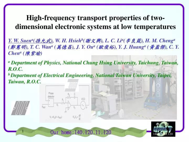
High-frequency transport properties of two-dimensional electronic systems at low temperatures. Y. W. Suen a ( 孫允武 ) , W. H. Hsieh b ( 謝文興 ), L. C. Li a ( 李良箴 ), H. M. Cheng a ( 鄭憲明 ), T. C. Wan a ( 萬德昌 ), J. Y. Ou a ( 歐俊裕 ), Y. J. Huang a ( 黃盈傑 ), C. Y. Chen a ( 陳紫瑜 )

E N D
High-frequency transport properties of two-dimensional electronic systems at low temperatures Y. W. Suena(孫允武), W. H. Hsiehb(謝文興), L. C. Lia(李良箴), H. M. Chenga (鄭憲明), T. C. Wana (萬德昌), J. Y. Oua (歐俊裕), Y. J. Huanga (黃盈傑), C. Y. Chena (陳紫瑜) a Department of Physics, National Chung Hsing University, Taichung, Taiwan, R.O.C.b.Department of Electrical Engineering, National Taiwan University, Taipei, Taiwan, R.O.C. 1 Our home:140.120.11.120
Samples: GaAs/AlGaAs: (1)交大電子 李建平 (2)以色列/彰師物理 吳仲卿 Si/SiGe: 台大凝態中心 鄭鴻祥 Instrumentaions: Pulsed RF/microwave PLL: 張冠英,陳家怜,王文凱,黃盈傑,李良箴 Cryogenic Systems, Wiring & Programming: 謝文興,李良箴,歐俊裕 Samples & Measurement:萬德昌,鄭憲明,謝文興,李良箴 Cheap Labor:陳紫瑜,歐俊裕 Money:NSC 2
Outline • Detection by a Phase Lock Loop • Surface Acoustic Wave Detector • Coplanar Wave Guide Detector • Pulsed Microwave PLL system • Some Preliminary Results • Kind of Conclusions • Future Works 4
Detection by Phase Lock Loop (PLL) f0 =f1+ fs =b1l1+bs(B)ls Df0 =0=Df1+Dfs(B) =Db1l1+Dbs(B)ls fs=bsls PLL system phase=f1=b1l1 sample Sample under detection B:the parameter (magnetic field) changed in the experimentu:velocity of the wave Dw can be measured very accurately. Type-II PLL 5
Reference From sample Keep at a constant phase difference Reference Df From sample Due to the change of sample conditions Reference Tuning the frequency to match the phase From sample 6
SAW Delay-Line Sensor L l GaAs:3.6×10⁻⁷W-1GaAs/LiNO3(Y-Z):1.8×10-6W-1 7
slower To get the same wave length (SAW), thus the same phase, one must decrease f. 8
SAW Delay-Line Sensor Df/f0 PSAW G Df/f0 B B B 9
Anything GOOD to use SAW detectors?! • No contact! • Short wavelength compared to EM signals at the same frequency. • Low energy compared to EM signals at the same wavelength. • We can use SAWs to detect the special length scale in the sample via the size-resonance of SAWs and the sample. 10
Coplanar Waveguide (CPW) Sensor 50Wmeandering CPWtotal length ls Electric field 11
Coplanar Waveguide (CPW) Sensor Some formulae: or 12
RF or Microwave Generator (A) DC-Coupled Frequency Modulation (FM) Integrator 積分器 黑色:低頻訊號 橙色:高頻訊號 Directional Couplers (I) (B) (b2) (b1) Double-Balance Mixer (M) PLL Precision Counter (C) (b3) Pulse Generator (P) High Speed Diode Switch Power Splitter (S) Time Delay Gated Average (s2) (s1) (D) (H) Power Detector (J) Step Attenuator Amplifier (E) (G) Intensity Output Stainless-Steal Semirigid Coax Stainless-Steal Semirigid Coax SAW Receiver IDT SAW Emitter IDT Sample Z Z (F) (F) Impedance Match Network Impedance Match Network Active LDES Region Cryogenic Environment Pulsed RF/Microwave PLL and Gated Averaging System • Why pulsed? • Use low average power to prevent from heating • Use gated averaging technique to avoid direct EM interruption • Avoid the reflection and multiple reflection signals What’s different from others: We use type II PLL, home-brew sample-&-hold circuits, and cheap lock-in amplifiers. 13
An improved homodyne amplitude detection scheme. Ref. Signal 0º 90º mixer To PLL 90º hybrid ~0 To amplitude detection Power splitter A home-made vector meter?? Signal from the sample 14
Signal Gating & Averaging: ~200 ms set by lock-in amp Peak power about –30dBm s1(t) RF/Microwave pulse train 0.2~2 ms set by pulse shaping circuit 3~4 ms set by lock-in amp s1(t) s2(t) signal of mixer or power detector time delay s4(t) signal after SH Direct coupled EM Reflected signals sampling delay set by pulse generator s3(t) fed into lock-in sampling gate set by a pulse generatorfed into the controlling node of a sample-and-hold circuit 15
A semiconductor chip attached on the SAW delay line Chip tied on the SAW delay line BeCu SR coax 5mm IDT SAW transducer He3 sample holder 17
Transmission of the SAW transducers Room temperature l=29mm 30 pairs 500mm Y-cut Z-propagation 18
Data read from SAW delay line (sample #1): ns=1.9×1011 cm-2 f0=120MHzT=0.3KGaAs/AlGaAs 2DES n=1 n=2 19
Data read from SAW delay line (sample #2): f0=120MHzT=0.3KGaAs/AlGaAs 2DES ns=2.5×1011 cm-2 20
Compared with :(SAW Data #1) sxx of sample #1 T=0.3 K 21
500ÅSi 3000 ÅSi 1.6×1012 cm-2(B doping) 100 Å_Si spacer_layer 300ÅSiGe 3000ÅSi buffer 5kW-Si substrate Transmission of the CPW transducer on Si/SiGe Width =25μmGap(deff) =43μmTransmission lenth = 13mm 24
Phys. Rev. So-Called Flows ofMW modules, Graduate students, ……….. 27
UnderConstruction^0^ 1. l<1mm e-beam writer Nano…..Nano…..Nano…..Nano…..Nano…..Nano…..Nano…..Nano…..Nano…..Nano….. 2. Acoustoelectric effect V or A spins 3. Quantum dots, spins, spintronics 4. Replace diode detectorwith……(homodyne det.) 29