Download
1 / 3
30 likes | 117 Views
EXPERIMENTAL DETAILS. veeco metal–organic chemical vapor deposition system Chip size 350*350µ MQW growth time are 1.5 nm (1 min), 2.0 nm (1.33 min), and 2.5 nm (1.67 min), respectively mounted onto TO-46 lead frames without epoxy encapsulation

E N D
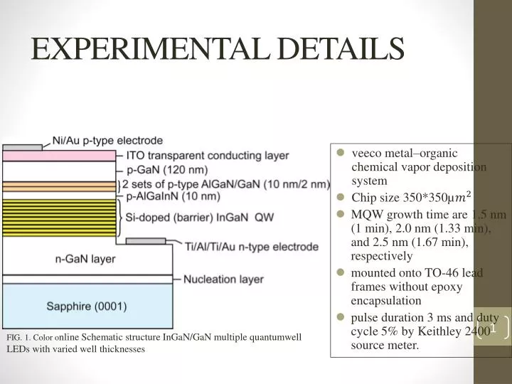
EXPERIMENTAL DETAILS • veeco metal–organic chemical vapor deposition system • Chip size 350*350µ • MQW growth time are 1.5 nm (1 min), 2.0 nm (1.33 min), and 2.5 nm (1.67 min), respectively • mounted onto TO-46 lead frames without epoxy encapsulation • pulse duration 3 ms and duty cycle 5% by Keithley 2400 source meter. FIG. 1. Color online Schematic structure InGaN/GaNmultiple quantumwellLEDs with varied well thicknesses
RESULTS AND DISCUSSION 2.9% 26.3% 43.8% Fig. 1. Normalized EQE measurements of the MQW LEDs with varied well thicknesses. A reduced efficiency droop behavior is demonstrated for the samples with thicker quantum wells. The inset shows absolute values of the external quantum efficiencies for the samples.
Fig. 2. Schematic figure of total current density Jtotal = Jrad + Jnrad+Joverflow. • Utilizing a commercial software—simulator of light emitters based on nitride semiconductors(SiLENSe)—is performed. • R