Download
1 / 25
250 likes | 274 Views
This presentation provides an overview of the key features of the Alpha 21264 microarchitecture, including its pipeline structure, fetch and branch prediction mechanisms, register renaming, and clustering.

E N D
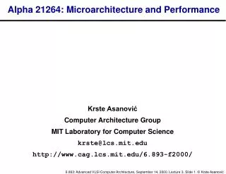
Alpha 21264 Microarchitecture Onur/Aditya 11/6/2001
Key Features of 21264 • Introduced in Feb 98 at 500 MHz • 15M transistors, 2.2V 0.35-micron 6 metal layer CMOS process • Implements 64-bit Alpha ISA • Out-of-order execution (unlike 21164) • 4-wide fetch (like 21164) • Max 6 inst/cycle execution bandwidth • 7-stage pipeline • Hybrid two-level branch prediction (tournament predictor) • Clustered integer pipeline • 80 in-flight instructions
Overview of the Presentation • Overview of 21264 pipeline • Fetch and Branch Prediction mechanism • Register Renaming in 21264 • Clustering • Memory System
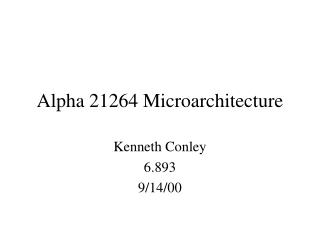
21264 Pipelines Source: Microprocessor Report, 10/28/96
Pipeline Structure Source: IEEE Micro, March-April 1999
Instruction Fetch Mechanism • Two features: • Line and way prediction • Branch prediction • Line-way predictor predicts the line-way of the I-cache that will be accessed in the next cycle • Line-way prediction takes the branch predictor outside the critical fetch loop. • On cache fills, line predictor value at each line points to the next sequential fetch line. • Line predictor is later trained by the branch predictor. • In effect, line-way predictor is similar to a very fast BTB. • Prediction of the line predictor is verified in stage 1 (Instruction slot). If line-way prediction is incorrect, slot stage is flushed and PC generated using the branch predictor information is used to redirect fetch.
Fetch - Line and Way Prediction Source: IEEE Micro, March-April 1999
Branch Prediction Mechanism • Hybrid Branch Predictor • Global predictor: • Good for inter-correlated branches. • Indexed by global path history register (T/NT status of last 12 branches) • 4K-entry table of 2-bit counters • Local Predictor • Good for self-correlated branches. • 10 bits of PC indexes a per-address local history table, which in turn indexes a 1K-entry table of 3-bit counters. • Aliasing among branches is a problem. • Choice Predictor • Decides which predictor to use. • Indexed by global path history register • 4K-entry table of 2-bit counters
Branch Prediction Mechanism • Minimum branch penalty: 7 cycles • Typical branch penalty: 11+ cycles (IQ delay) • 48K bits of target addresses stored in I-cache • 32-entry return address stack • Predictor tables are reset on a context switch Source: Microprocessor Report, 10/28/96
Instruction Slotting • Check line predictor prediction • Branch predictor compares the next cache index it generates with the one generated by line predictor • Determine the subclusters integer instructions will go to • Some subclusters are specialized resource constraints • Perform load balancing on subclusters
Register Renaming • 31 Integer 31 FP architectural registers • 41 Int 41 FP extra physical registers • Uses a merged rename and architectural register file, one for Int one for FP • Same physical register holds the results of an instruction before and after commit • No separate architectural register file (no data copying on commit) • Register map table stores current mappings of architectural registers. • A map silo contains old mappings of up to 20 previous decode cycles (used in case of misprediction)
Register Renaming Logic • On decoding an instruction: • Search map CAMs for the source registers • Find the physical registers currently containing the value of the architectural source registers • Access free physical register list • Map the found free physical register to the architectural destination register Source: Presentation by R. Kessler, August 1998.
Register Renaming Logic • On completing an instruction: • Write result into the physical destination register • Mark the physical destination register as valid in the register scoreboard • Broadcast results to issue queue entries • Physical destination register number is broadcast as tag • On committing an instruction • Mark the physical destination register as committed • Free the physical register that corresponds to an old mapping of the same architectural register • On a misprediction/exception • Roll back the map state to what it was when the exception-causing instruction was renamed • To be able to do this, instructions should be associated with map entries • This is done using inums. Each instruction is given an 8-bit unique identifier during register mapping
Physical Register States • 4 states • Initially n architectural registers are in AR state. • Rest are Available • When an instruction with a destination register is issued, one of the available registers is allocated as rename buffer (RB) • When instruction finishes execution, state is set to valid • On instruction commit, state is set to AR and old AR mapping is reclaimed Source: Sima, D. The Design Space of Register Renaming Techniques. IEEE Micro, September/October 2000.
Integer Issue Queues - Clustering • 20 entries, maximum 4 per cycle • Two arbiters pick the instructions that will issue (One for upper subclusters, one for lower subclusters) • Each queue entry asserts a request to the arbiter when it contains an instruction that can be executed by the subcluster (if operand values are available within that subcluster) • 4 request signals (U0, U1, L0, L1) • Arbiters choose between simultaneous requesters of a subcluster based on the age of the request • Older instructions are given priority • Each arbiter picks 2 of the possible 20 requesters for service • A given instruction can request only upper or lower subclusters (load balancing based on the assignment done by Stage 1) • Subcluster assignment is static (Stage 1) • Cluster selection on issue is dynamic (Stage 2)
Integer/FP Execution Pipes • Integer cluster communication latency: 1 cycle • Advantage of clustering: • Fewer read/write ports to the register file • Register file will not be a cycle time limiter • FP issue queue: • 15 entries • 2 inst/cycle Source: IEEE Micro, March-April 1999
Memory References • Load Queue • Reorder buffer for loads • 32 entries, in-order • Maintains state of loads issued but not yet retired • Store Queue • Reorder buffer for stores • 32 entries, in-order • Maintains state of stores issued but not yet written to the data cache • Holds data associated with store instructions • Forwards data to older matching stores • Miss Address File • Holds physical addresses associated with pending L1 cache misses (instruction or data) • Maximum 8 misses to off-chip memory system
Load/Store Ordering • New memory references check their address and age against older references. • For example, when a store issues: • LDQ compares store address to the addresses of younger loads (CAM search) • If the older store issues to the same memory address as a younger load, LDQ squashes the load and initiates recovery • When a load is ready to issue: • STQ compares the load address to the addresses of younger stores • If a match is found: • If store data is available, STQ forwards the data • Else load issue is delayed until store data becomes available
Load/Store Ordering • When a load is ready to issue: • If a younger store exists in STQ with an unknown address: • Predict that the ready load will not access the same memory location unless this load was incorrectly ordered before (check the load wait table) • Exposes more ILP if prediction is correct • In case of misprediction: • Minimum 14 cycle penalty • Initiate recovery: Load and all subsequent instructions are squashed and re-executed • Mark the load in the load wait table so that it will wait for all younger stores to compute addresses next time around
Load/Store Ordering Example Source: IEEE Micro, March-April 1999
Features of Memory System • Data cache • 64 KB, 2-way, virtually-indexed physically tagged (translation in parallel with access) • Write-back, read/write allocate • 64-byte block size + ECC bits • Prevents synonyms by not allowing different physical addresses corresponding to the same virtual address to co-exist in the cache • Load hit/miss prediction to minimize load-use latency (Data cache access is 3 cycles after the issue queue + 1 cycle to get the hit/miss signal to issue queue) • Victim Buffer (Victim address and data files) • Contains evicted L1(Data and Inst) and L2 cache lines • 8 entries, Serial access • Off-chip L2 cache • Minimum data cache miss latency 13 cycles • Up to 16 MB • Dedicated access to L2 cache
Overall System Diagram Source: Microprocessor Report, 10/28/96
References • R.E. Kessler. The Alpha 21264 Microprocessor. IEEE Micro. March/April 1999. • D. Leibholz and R. Razdan. The Alpha 21264: A 500 MHz Out-of-order Execution Microprocessor. COMPCON97, 1997. • Compaq Computer Corporation. Alpha 21264/EV6 Hardware Reference Manual. • R. Kessler, E. McLellan, and D. Webb. The Alpha 21264 microprocessor architecture. International Conference on Computer Design, October 1998 • B.A. Gieseke et. al. A 600 MHz Superscalar RISC Microprocessor with Out-of-order Execution. International Solid State Circuits Conference. 1997. • L. Gwennap. Digital 21264 Sets New Standard. Microprocessor Report. October 28, 1996. • Dezso Sima. The Design Space of Register Renaming Techniques. IEEE Micro. September/October 2000. • P.E. Gronowski et.al. High Performance Microprocessor Design. IEEE Journal of Solid State Circuits. May 1998.