Download
1 / 20
200 likes | 295 Views
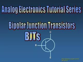
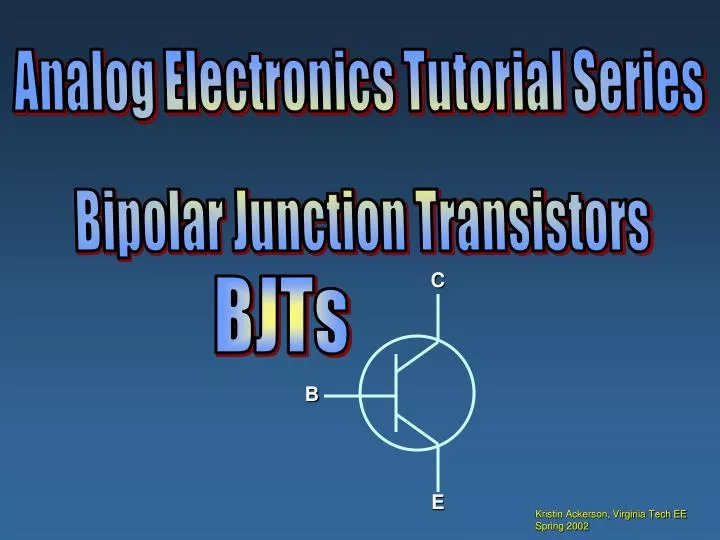
Analog Electronics Tutorial Series Bipolar Junction Transistors. C. BJTs. B. E. Kristin Ackerson, Virginia Tech EE Spring 2002. Table of Contents. The Bipolar Junction Transistor_______________________________slide 3 BJT Relationships – Equations________________________________slide 4

E N D
Analog Electronics Tutorial Series Bipolar Junction Transistors C BJTs B E Kristin Ackerson, Virginia Tech EE Spring 2002
Table of Contents The Bipolar Junction Transistor_______________________________slide 3 BJT Relationships – Equations________________________________slide 4 DC and DC _____________________________________________slides 5 BJT Example_______________________________________________slide 6 BJT Transconductance Curve_________________________________slide 7 Modes of Operation_________________________________________slide 8 Three Types of BJT Biasing__________________________________slide 9 Common Base______________________slide 10-11 Common Emitter_____________________slide 12 Common Collector___________________slide 13 Eber-Moll Model__________________________________________slides 14-15 Small Signal BJT Equivalent Circuit__________________________slides 16 The Early Effect___________________________________________slide 17 Early Effect Example_______________________________________slide 18 Breakdown Voltage________________________________________slide 19 Sources__________________________________________________slide 20 Kristin Ackerson, Virginia Tech EE Spring 2002
The BJT – Bipolar Junction Transistor Note: It will be very helpful to go through the Analog Electronics Diodes Tutorial to get information on doping, n-type and p-type materials. The Two Types of BJT Transistors: npn pnp n p n p n p E C E C C C Cross Section Cross Section B B B B Schematic Symbol Schematic Symbol E E • Collector doping is usually ~ 106 • Base doping is slightly higher ~ 107 – 108 • Emitter doping is much higher ~ 1015 Kristin Ackerson, Virginia Tech EE Spring 2002
BJT Relationships - Equations IE IC IE IC - VCE + + VEC - E C E C - - + + VBE VBC IB VEB VCB IB + + - - B B npn IE = IB + IC VCE = -VBC + VBE pnp IE = IB + IC VEC = VEB - VCB Note: The equations seen above are for the transistor, not the circuit. Kristin Ackerson, Virginia Tech EE Spring 2002
DC and DC = Common-emitter current gain = Common-base current gain = IC = IC IB IE The relationships between the two parameters are: = = + 1 1 - Note: and are sometimes referred to as dc and dc because the relationships being dealt with in the BJT are DC. Kristin Ackerson, Virginia Tech EE Spring 2002
BJT Example Using Common-Base NPN Circuit Configuration C • Given: IB = 50 A , IC = 1 mA • Find: IE , , and • Solution: • IE = IB + IC = 0.05 mA + 1 mA = 1.05 mA • = IC / IB = 1 mA / 0.05 mA = 20 = IC / IE = 1 mA / 1.05 mA = 0.95238 could also be calculated using the value of with the formula from the previous slide. = = 20 = 0.95238 + 1 21 IC VCB + _ IB B VBE IE + _ E Kristin Ackerson, Virginia Tech EE Spring 2002
BJT Transconductance Curve Typical NPN Transistor 1 Collector Current: IC = IESeVBE/VT Transconductance: (slope of the curve) gm = IC / VBE IES = The reverse saturation current of the B-E Junction. VT = kT/q = 26 mV (@ T=300K) = the emission coefficient and is usually ~1 IC 8 mA 6 mA 4 mA 2 mA VBE 0.7 V Kristin Ackerson, Virginia Tech EE Spring 2002
Modes of Operation Active: • Most important mode of operation • Central to amplifier operation • The region where current curves are practically flat Saturation: • Barrier potential of the junctions cancel each other out causing a virtual short Cutoff: • Current reduced to zero • Ideal transistor behaves like an open switch * Note: There is also a mode of operation called inverse active, but it is rarely used. Kristin Ackerson, Virginia Tech EE Spring 2002
Three Types of BJT Biasing Biasing the transistor refers to applying voltage to get the transistor to achieve certain operating conditions. Common-Base Biasing (CB) : input = VEB & IE output = VCB & IC Common-Emitter Biasing (CE): input = VBE & IB output = VCE & IC Common-Collector Biasing (CC): input = VBC & IB output = VEC & IE Kristin Ackerson, Virginia Tech EE Spring 2002
Common-Base Although the Common-Base configuration is not the most common biasing type, it is often helpful in the understanding of how the BJT works. Emitter-Current Curves IC Active Region IE Saturation Region Cutoff IE = 0 VCB Kristin Ackerson, Virginia Tech EE Spring 2002
Common-Base VCE IC IE C E VCB VBE IB + _ + _ B VCB VBE Circuit Diagram: NPN Transistor The Table Below lists assumptions that can be made for the attributes of the common-base biased circuit in the different regions of operation. Given for a Silicon NPN transistor. Kristin Ackerson, Virginia Tech EE Spring 2002
Common-Emitter Circuit Diagram Collector-Current Curves VCE IC IC + _ Active Region VCC IB IB VCE Saturation Region Cutoff Region IB = 0 Kristin Ackerson, Virginia Tech EE Spring 2002
Common-Collector Emitter-Current Curves IE The Common-Collector biasing circuit is basically equivalent to the common-emitter biased circuit except instead of looking at IC as a function of VCE and IB we are looking at IE. Also, since ~ 1, and = IC/IE that means IC~IE Active Region IB VCE Saturation Region Cutoff Region IB = 0 Kristin Ackerson, Virginia Tech EE Spring 2002
Eber-Moll BJT Model The Eber-Moll Model for BJTs is fairly complex, but it is valid in all regions of BJT operation. The circuit diagram below shows all the components of the Eber-Moll Model: IE IC E C RIC RIE IF IR IB B Kristin Ackerson, Virginia Tech EE Spring 2002
Eber-Moll BJT Model R = Common-base current gain (in forward active mode) F = Common-base current gain (in inverse active mode) IES = Reverse-Saturation Current of B-E Junction ICS = Reverse-Saturation Current of B-C Junction IC = FIF – IR IB = IE - IC IE = IF - RIR IF = IES [exp(qVBE/kT) – 1] IR = IC [exp(qVBC/kT) – 1] If IES & ICS are not given, they can be determined using various BJT parameters. Kristin Ackerson, Virginia Tech EE Spring 2002
Small Signal BJT Equivalent Circuit The small-signal model can be used when the BJT is in the active region. The small-signal active-region model for a CB circuit is shown below: iB iC B C r iB r = ( + 1) * VT IE iE E @ = 1 and T = 25C r = ( + 1) * 0.026 IE Recall: = IC / IB Kristin Ackerson, Virginia Tech EE Spring 2002
The Early Effect (Early Voltage) IC Note: Common-Emitter Configuration IB -VA VCE Green = Ideal IC Orange = Actual IC (IC’) IC’ = IC VCE + 1 VA Kristin Ackerson, Virginia Tech EE Spring 2002
Early Effect Example Given: The common-emitter circuit below with IB = 25A, VCC = 15V, = 100 and VA = 80. Find: a) The ideal collector current b) The actual collector current Circuit Diagram VCE IC • = 100 = IC/IB a) IC = 100 * IB = 100 * (25x10-6 A) IC = 2.5 mA + _ VCC IB b) IC’ = IC VCE + 1 = 2.5x10⁻³ 15 + 1 = 2.96 mA VA 80 IC’ = 2.96 mA Kristin Ackerson, Virginia Tech EE Spring 2002
Breakdown Voltage The maximum voltage that the BJT can withstand. BVCEO = The breakdown voltage for a common-emitter biased circuit. This breakdown voltage usually ranges from ~20-1000 Volts. BVCBO = The breakdown voltage for a common-base biased circuit. This breakdown voltage is usually much higher than BVCEO and has a minimum value of ~60 Volts. • Breakdown Voltage is Determined By: • The Base Width • Material Being Used • Doping Levels • Biasing Voltage Kristin Ackerson, Virginia Tech EE Spring 2002
Sources Dailey, Denton. Electronic Devices and Circuits, Discrete and Integrated. Prentice Hall, New Jersey: 2001. (pp 84-153) 1 Figure 3.7, Transconductance curve for a typical npn transistor, pg 90. Liou, J.J. and Yuan, J.S. Semiconductor Device Physics and Simulation. Plenum Press, New York: 1998. Neamen, Donald. Semiconductor Physics & Devices. Basic Principles. McGraw-Hill, Boston: 1997. (pp 351-409) Web Sites http://www.infoplease.com/ce6/sci/A0861609.html Kristin Ackerson, Virginia Tech EE Spring 2002