Download
1 / 7
70 likes | 220 Views
TYPICALLY REALIZABLE COMPONENTS IN MICS. Passive components Low pass,high pass Band pass,band stop with medium to large bandwidths Directional couplers Power splitters Power combiners Circulators,isolators(with ferrite substrates) Attenuators Resonators Transformer circuits Branches

E N D
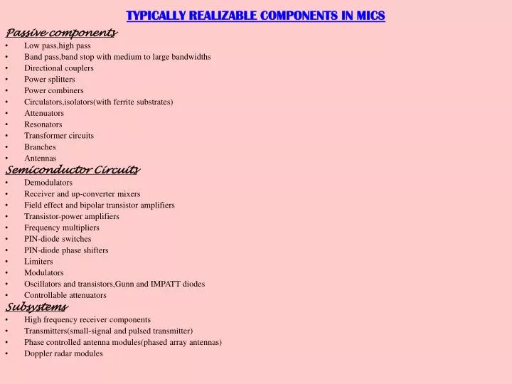
TYPICALLY REALIZABLE COMPONENTS IN MICS Passive components • Low pass,high pass • Band pass,band stop with medium to large bandwidths • Directional couplers • Power splitters • Power combiners • Circulators,isolators(with ferrite substrates) • Attenuators • Resonators • Transformer circuits • Branches • Antennas Semiconductor Circuits • Demodulators • Receiver and up-converter mixers • Field effect and bipolar transistor amplifiers • Transistor-power amplifiers • Frequency multipliers • PIN-diode switches • PIN-diode phase shifters • Limiters • Modulators • Oscillators and transistors,Gunn and IMPATT diodes • Controllable attenuators Subsystems • High frequency receiver components • Transmitters(small-signal and pulsed transmitter) • Phase controlled antenna modules(phased array antennas) • Doppler radar modules
FUNCTIONAL COMPONENTS OF A MIC ( FROM A VIEWPOINT OF A CIRCUIT DEVELOPER ) Electrical functional units • Straight-line striplines(e.g. microstrip,coplanar lines) • Stripline discontinuities(e.g. branches,bends,open and short circuits) • Concentrated reactive components:capacitors,inductors • Circuit terminations • High frequency resistances(e.g. attenuators) • Resistors in bias supplies for semiconductors • Semi conductors:diodes,transistors • Special components(e.g. circulators,dielectric,resonators,stripline,antennas) Mechanical functional units • Housing • High frequency connections • Dc connections
STRUCTURAL COMPONENTS OF A MIC OF A THIN-FILM HYBRID TYPE( AS SEEN FROM THE TECHNOLOGICAL STANDPOINT ) Layered Circuit • Substrate • Integrated elements: Conductor structure Resistor structure(with or without alignment) (Laminated capacitors) • Hybrid elements: Capacitors(e.g. ceramic chips and beam lead capacitors) Semiconductors:diodes,transistors(with or without packaging) Trimmer capacitors and resistors Circulators(inserted ferrite disks) Dielectric resonators(HDK ceramic blocks) Semiflexible miniature coaxial lines • Connector sections(wires,bands) • Substrate openings(holes for through-contacts,notches) • Plastic coverings and protective covers for sensitive hybrid elements Packaging • Individual housing ( hermetically sealed or not) • High frequency connectors,substrate to substrate connections • Dc connections(lead through capacitors)
COMPARISON WITH THIN-FILM HYBRID CIRCUIT • As compared with Al2O3 ceramic thin-film circuits GaAs MMICs have the following properties: • Higher upper limiting frequencies and wider possible bandwidths due to low reactive interconnections; • Better reproducibility of performance due to the lack of wire and band connections in the circuit; • Higher packing density,smaller substrate sizes,higher miniaturization,higher number of circuits(up to 100 per large substrate) in volume production; • Cheaper for larger production runs; • No adjustment possible; • Slightly smaller choice of semiconductor components(e.g. no IMPATTs) but includes the possibility of new circuit concepts(active transistor matching,active mixers); • Investment in equipment necessary; • Harder to develop circuits,so computer aided design(CAD) is essential.
Required property Mechanical carrier for the circuit Mechanical stability(“robustness”)(e.g. against breakage) Maintenance of shape(no cold flow) High thermal conductivity Long term stability against environment(temperature changes,high and low temperature storage,dampness,industrial waste gases) Thermal expansion similar to that of metals Small dimensional variations Wave conducting medium High er(10-20) Er homogeneity Small variation in er from sample to sample Minimum variation of er with temperature Low dielectric loss(tan(delta e) < 0.001)at microwave frequencies No water absorption High specific resistance p>10^10ohms cm Small variations in thickness(within a substrate and from sample to sample) Reason Mechanical loads upon equipment due to shock and vibration during use Stable package mounting Heat removal from components(e.g. power transistors) Reliability of the circuit Reliable packaging(e.g. soldering) over entire operating temperature range Precise fit in housing to avoid parasitic reactance at connector Size reduction(high wavelength reduction factor) Homogenous circuit parameters Reproducible production qualities Low temperature dependence of filters and resonators Low loss circuits,high Q Maintenance of circuit operation in damp air Low loss circuits Reproducibility of circuit parameters CRITERIA FOR THE CHOICE OF SUBSTRATE MATERIAL IN THIN FILM USES
High electrical insulation strength Technological medium Stability at high temperatures(1000-2000 degree C) Chemical reactance Flat surface,low cambering Smooth surface(indentation depth sigmaeff < 0.5 micro m,core size < 1 micro m) Easily workable(drilling and separating) Maintenance of shape under pressure Surface without defects(e.g. pin holes) Thermal expansion coefficient similar to that of conductor material Commercial and Manufacturing criteria Low cost Easy to store Safe to machine Generally available Delivering in large plates Circuits for high powers For thin film and thick film technologies and soldering(not for simple etching technologies) For photo etching techniques For high structural accuracy when using photomasks For high adhesion of thin film conductors Through contacts,cutting,and preparation For thermo compression and ultra sonic bonding For thin film capacitors Adhesion of conductors Low production costs Low production costs Low production costs Low production costs Economical production