Download
1 / 24
320 likes | 931 Views
Materials: Electrical and Mechanical Properties. EE485A Lecture 1, 3 September 2009. Electrical classifications. Metals Easily conduct electricity Al, Cr, Au, Pt, Ni, Ti all common in MEMS Insulators Do not conduct electricity SiO2, Si3N4, Al2O3 common in MEMS Semiconductors

E N D
Materials: Electrical and Mechanical Properties EE485A Lecture 1, 3 September 2009
Electrical classifications • Metals • Easily conduct electricity • Al, Cr, Au, Pt, Ni, Ti all common in MEMS • Insulators • Do not conduct electricity • SiO2, Si3N4, Al2O3 common in MEMS • Semiconductors • Conductivity can be controlled over wide range by material processing. • Electrical properties derive from crystal structure
Crystal Structure Simple Cubic Body-Centered Cubic Face-Centered Cubic
Si crystal structure • Appears like two fcc crystals offset by 1/4 of body diagonal
a z a x y Crystal planes and orientation • Characterized by Miller Indices • Identify intercepts of plane with x, y, and z axes • Take the reciprocals of these numbers and reduce to the smallest set of integers h, k and l. • Example: • Resources on-line: http://chemistry.bd.psu.edu/jircitano/Miller.html http://www.doitpoms.ac.uk/tlplib/miller_indices/index.php ID Intercepts: a, a, Take reciprocal: Reduce to smallest set of integers:
Problems If the lattice constant, a, of Silicon is 5.43Å, determine the nearest neighbor distance 5.43 Å
Problems A particular bcc crystal has a lattice constant of 4 Å, determine the density of the crystal in terms of atoms/cm3
Problems On the figures below, sketch the (1,0,0) and (1, 1, 1) planes
Electrons and Holes • Notice that Si has 4 nearest neighbors • Leads to happy covalent bonding • Thermal energy breaks some bonds, creating “free” electrons and “holes” • In intrinsic silicon, the number of “free” electrons equals the numbers of holes Intrinsic carrier concentration For Si at room temp: ni = 1.5 x 1010 cm-3 concentration of electrons (#/cm3 or cm-3) concentration of holes (cm-3)
Extrinsic Semiconductors • Atoms introduced to lattice that have either 3 or 5 valence electrons instead of 4. + P-type doping: Dopants introduce holes and fixed negative ions N-type doping: Dopants introduce “free” electrons and fixed positive ions
Extrinsic carrier concentrations • At thermal equilibrium, np = ni2 even for doped semiconductors • Given donor (n-type) doping conc., ND and acceptor (p-type) doping conc. NA: • ND >> NA : • NA >> ND : • NA ~ ND : Solve the following equations simultaneously:
Conductivity and Resistivity • Both “free” electrons and holes conduct • Resistivity, r[W·cm], given by: s = conductivity q = charge of an electron (1.6E-19 C) mn = electron mobility (Si at room temp ~ 1350 cm2/V-s) mp = hole mobility (Si at room temp ~ 480 cm2/V-s) • Resistance [W] and Sheet Resistivity [W/]: L I direction t W
Problems Given Si at room temp with NA = 1016, calculate • n, p, r • Sheet resistivity for 100 nm thick layer • Resistance if 1 mm wide and 10 mm long
Stress and Strain • Newton’s Laws of Motion • First Law: The law of inertia (every object in motion remains in motion unless an external force is applied) • Second Law: F = ma • Third Law: For every action, there is an equal and opposite reaction • For any stationary object, the vector sum of the forces and moment (torque) on the object and on any part of it must be zero. • Stress: Intensity of force (force/area) acting on a structure or portion of a structure • Strain: Response of structure to stress (elongation/unit length)
F F F F F Since bar is in equilibrium, every portion of the bar is also in equilibrium Free-Body Diagrams • Consider bar embedded in brick wall with axial force F applied to end. • Free-body diagram: pictorial representation used for analysis that shows all forces acting on an object. L If the bar is stationary, the wall must produce a reaction force equal and opposite to the applied force. F F
Free-Body Diagram with Torque Reactive torque (or “moment”) balances torque created by applied force at beam tip F L L” L’ F M= FL F F F F M= FL’ F M= FL M= FL’
Normal Stress • Consider a rod being pulled axially with force F F A F The force is continuously distributed through the device, and at any cross-section, the intensity of the force perpendicular the cross-section is given by the normal stress, s.
Normal Strain • Under axial tension, the rod length will increase, and the cross-sectional area will decrease. H0-DH H0 L0 W0-DW L0+DL W0 Normal strain, sx = Strain in transverse dimensions, sy and sz: Transverse strain related to longitudinal strain by Poisson’s Ratio, n:
Hooke’s Law • Stress and strain related through modulus of elasticity (Young’s Modulus), E (units: force/area): • Stiffer materials have a larger Young’s Modulus. • Mechanical properties of common MEMS materials given in Appendix A (p. 517)
Class Exercises A 500 mm-long silicon beam that is 50 mmwide and 1 mm thick is pulled longitudinally with a force of 1 N. Determine the normal stress, the normal strain, the resulting beam length and cross-sectional area. For Silicon, E = 130 GPa and n = 0.25.
Shear Stress and Strain • Shear stresses are created when torque is applied to an object, and they work to change the shape of the element Area, A DX F L F Shear stress magnitude [N/m2]: G, E, and n all related by: Shear strain [unitless]: Shear stress and strain related by shear modulus of elasticity, G [N/m2]:
Class Exercise A gold beam that is 500 mm long, 50 mm thick and 50 mm wide experiences a shear stress of 100 MPa on its top and bottom surfaces. Determine the magnitude of force required to cause this, the shear strain and the resulting DX. For Gold, E= 78 GPa, and n = 0.42.
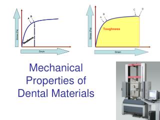
Stress vs. Strain in General Fracture Point stress Yield stress Proportional limit Hooke’s Law Applies in Elastic Regime Only strain Necking Strain Hardening Yielding Elastic Regime Plastic Regime
General Stress Strain Relations • Stress-strain relationships can be orientation dependent. Normal stresses Normal strain Shear stresses Shear strain “Stiffness Matrix” (inverse of compliance matrix)