Download
1 / 9
90 likes | 204 Views
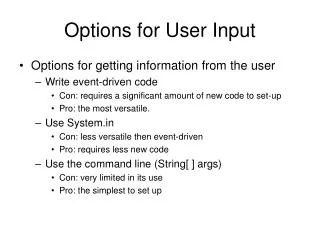
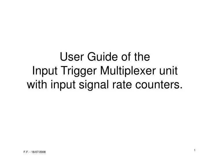
User Guide of the Input Trigger Multiplexer unit with input signal rate counters. Rx Low card configuration. rxCH1 rxCH2 rxCH3 rxCH4 rxCH5 rxCH6 rxCH7 rxCH8 rxCH9 rxCH10 rxCH11 rxCH12 rxCH13. rxCH14 rxCH15 rxCH16 rxCH17 rxCH18 rxCH19 rxCH20 rxCH21 rxCH22 rxCH23 rxCH24

E N D
User Guide of theInput Trigger Multiplexer unitwith input signal rate counters. F.F. - 18/07/2008
Rx Low card configuration rxCH1 rxCH2 rxCH3 rxCH4 rxCH5 rxCH6 rxCH7 rxCH8 rxCH9 rxCH10 rxCH11 rxCH12 rxCH13 rxCH14 rxCH15 rxCH16 rxCH17 rxCH18 rxCH19 rxCH20 rxCH21 rxCH22 rxCH23 rxCH24 rxCH25 LSB MSB Base address range: 1F-00 NOTE: For Rx High card the only change concerns the rxCH number sequence: rxCH1 becomes rxCH26 rxCH2 becomes rxCH27 …… ……. …… rxCH25 becomes rxCH50 Termination resistor jumpers External CLK (daisy chain) F.F. - 18/07/2008
TxMux card configuration txCH1 txCH2 txCH3 txCH4 txCH5 txCH6 txCH7 txCH8 txCH9 txCH10 txCH11 txCH12 txCH13 txCH14 txCH15 txCH16 txCH17 txCH18 txCH19 txCH20 txCH21 txCH22 txCH23 txCH24 txCH25 Base address range: 1F-00 External CLK (daisy chain) LSB MSB F.F. - 18/07/2008
FI card FI card GA=3 (2nd TxMux card) GA=0 (1st TXMux card) GA=2 (Rx High card) GA=1 (Rx Low card) Auxiliary P2 Backplane slots (as seen from front of crate when plugged) • The auxiliary backplane is 4 slot wide and is plugged on the rear side of P2. • The 4 locations are identified by their Geographical Address pins (GA): • GA=0 is used by a 1st TxMux card • GA=1 and GA=2 are used for Rx cards • GA=3 is used by a 2nd TxMux card • The two rightmost locations are used by the trigger FanIn cards (no VME addressing space) F.F. - 18/07/2008
Register 1 … 50 Register 0 = OFF 1 … 50 0 = OFF IN rate counter (r/o by VME) IN rate counter (r/o by VME) Logic diagram Rx High card 50 rxCH50 1st TxMux card 50 txCH25 txCH1 26 rxCH26 1 LHC CLK (external) GA = 2 LHC CLK (external) Each Rx input channel has a rate counter that is operated by a dedicated 32 bit register GA = 0 Each TxMux output channel has a 50 input multiplexer that is operated by a dedicated 6 bit register Rx Low card 2nd TxMux card 25 rxCH25 50 txCH25 txCH1 1 rxCH1 1 LHC CLK (external) GA = 1 LHC CLK (external) GA = 3 UD pins on auxiliary bus (P2 connector and backplane) F.F. - 18/07/2008
VME space • Rx and TxMux cards are automatically selected by plugging them into the dedicated GA slots (note however that Rx cards require manual insertion of terminator resistor jumpers – see page 2) • Rx Low and High cards do not require software configuration download for the Trigger Signal routing. • Rx cards need configuration to enable and select the IN Rate Counters. By default or reset all 25 counters are switched OFF. Eight types of counting can be selected (see details at page 8). • An external clock source (LHC CLK) is necessary if counting has to be synchronized with the experiment system clock. The input is at the front panel; it requires a NIM signal and a 50Ω termination at the end of the daisy chained cable. The selection from internal free running clock and the external synchronous clock is done automatically by the RX card (while an external clk signal is provided, the external clk is selected). • The phase of the external LHC CLK can be adjusted by VME in four steps of 90 degrees. • Tx Mux card 1 (i.e. plugged into GA=0) inverts the outputs, while Tx Mux card 2 (i.e. plugged into GA=3) does not invert the outputs. • VME address space: • A24/D32 • Base Addresses = from 1F00xxHex to 0000xxHex selectable by switches • Internal register addresses = from 00Hex to 64Hex (00, 04, 08, …, 60, 64) F.F. - 18/07/2008
VME space • Description of Register 00 (control/status) for both Rx and TxMux cards: • Write: bits 06, 05 = LHC_CLK Phase select (four steps of ¼ of period) • bit 0 = s/w reset -> puts the TxMux card in OFF state, i.e. all channels disabled • -> puts the Rx card in OFF state, i.e. all counters disabled • -> puts the external clock phase to 0 degrees • Read: bit 07 = ON when PLL is unlocked • bits 06, 05 = 0,0 => phase 0 degrees • 0,1 => phase 90 degrees • 1,0 => phase 180 degrees • 1,1 => phase 270 degrees • bit 04 = ON when LHC Clock is active (automatic selection by providing external clk) • bit 3 = ON when Rx High card • bit 2 = ON when Rx Low card • bit 1 = ON when TxMux card • bit 0 = ON for last s/w reset action, OFF after first read F.F. - 18/07/2008
VME space • Description of Registers 04Hex (txCH1) to 64Hex (txCH25) (multiplexer selection) for TxMux cards only: • Write/Read: bit 5 to bit 0 = selection of input channel (1 to 50) • (0, reset default = OFF; nn = select rx channel nn) • Description of Registers 04Hex (cntCH1) to 64Hex (cntCH25) for Rx cards only: • Write/Read: bit 31 to bit 28 = selection of counting type • Counting types: 0 => counting OFF (reset default) • 5 => counts pulses with width < 1 period • 6 => counts pulses with width ≥ 1 period • 7 => counts pulses with width = 1 period • A => counts pulses with width ≥ 2 periods • B => counts pulses with width = 2 periods • E => counts pulses with width ≥ 3 periods • F => counts pulses while level in ON • Read only: bit 25 to bit 0 = rate counter values (updated every second) F.F. - 18/07/2008
Front Panel Reset = ON when operating manual reset button VME Write = ON when TxMux card VME Read = ON when Rx card (Low or High) PLL Locked = ON when card selected by VME or reset by Power ON, SYSRST, Push button, S/W reset External clock inputs LEMOs (NIM logic) are used if external synchronous clock is required. This option is useful if users want synchronizing the rate counters to the LHC experiment system clock. F.F. - 18/07/2008