Download
1 / 40
530 likes | 821 Views
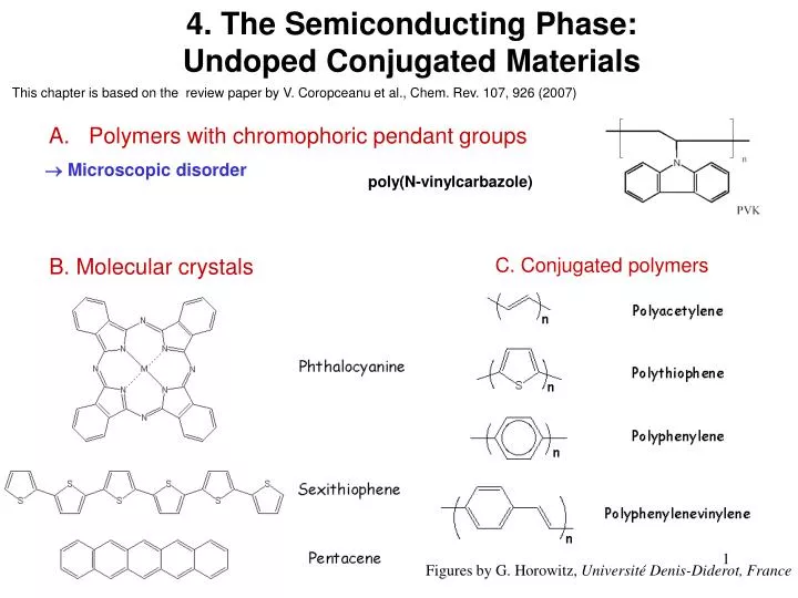
4. The Semiconducting Phase: Undoped Conjugated Materials. This chapter is based on the review paper by V. Coropceanu et al., Chem. Rev. 107, 926 (2007). Microscopic disorder. Polymers with chromophoric pendant groups poly(N-vinylcarbazole). B. Molecular crystals.

E N D
4. The Semiconducting Phase: Undoped Conjugated Materials This chapter is based on the review paper by V. Coropceanu et al., Chem. Rev. 107, 926 (2007) Microscopic disorder • Polymers with chromophoric pendant groups poly(N-vinylcarbazole) B. Molecular crystals C. Conjugated polymers Figures by G. Horowitz, Université Denis-Diderot, France
4.1. Organic semiconductors among other solids σ = electrical conductivity Eg = Band gap 1 S (Siemens)=1/ Ω For Eg> ~2eV Insulator σRT< 10-10Ω-1cm-1= 10-10 S/cm For 0< Eg < 2eV Semiconductor 10-10 S/cm < σ RT < 102 S/cm For Eg0 Metal σRT > 102 S/cm
E 4.1.1. Definitions The mobility of the charge carriers is the average speed of diffusion ||, or net drift velocity, of the charge carrier (cm/s) as a function of applied electric field (V/cm) = ||/E in cm2/Vs is positive even though e- and h+ travel in opposite direction. || The electrical conductivity σ can be defined as a sum of two terms: σ= (ne e + pe h ) in 1/Ωcm n and p = density of charge carriers (n for electrons and p for holes) in cm-3 e = unitary charge (C)
4.1.2. Temperature dependence The behavior of the electrical conductivity () vs. In a simplified manner, the temperature (T) of solids is one criterion used to classify them as: metal: decreases as T is raised semiconductor: increases as T is raised Note that an insulator appears as a semiconductor with very low conductivity. Metals chem/kT The excitation energy can be provided via an increase of temperature. The population of the orbitals is given by the Fermi-Dirac distribution: chem is the electron chemical potential, that is -EF for metals (T=0) When T increases, the charge carrier density increases…. However the conductivity decreases because there are more collisions between the transported electrons and the nuclei (phonon scattering) less efficient transport.
Semiconductors In order to have a net electrical current: electrons must jump from filled levels to empty levels across the band gap If Eg is not too large, upon applying an external electric field, few electrons at room T have the necessary energy to jump from valence band to conduction band Thermal energy: kT; at 300K, kT~0.025 eV~0.6 kcal/mol In crystals of intrinsic inorganic semiconductors, the band gap can be small, thermal excitations promote e- to the conduction band. The concentration in charge carriers produced is proportional to exp(-Eg/2kBT), leading to an increase of σ with T. The delocalized electrons/holes are not strongly bound to each other because of the high dielectric constant and participate efficiently to the electrical current. In undoped conjugated polymers, Eg is large. So, the thermal excitation are negligible, i.e the concentration of carrier does not increase with T. However, the conductivity increases with T like in organic crystals. This is the subject of this chapter.
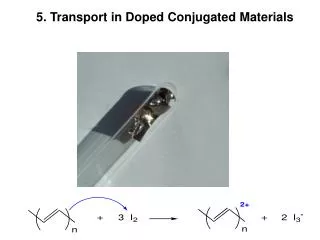
4.1.3. Undoped Conjugated Polymers • From the order of magnitude of the band gap and the conductivity, most undoped conjugated polymers are rather like ”insulators”. • However, these organic polymers do have a conjugated π-system. The formation of occupied π-valence band and π*-conduction band results in a lower band gap. As a result, they have a low ionization potential (IP) (usually lower than ~6eV) and/or a high electron affinity (EA) (lower that ~2eV) They will be easily oxidized by electron accepting molecules (I2, AsF5, SbF5,…) and/or easily reduced by electron donors (alkali metals: Li, Na, K) Charge transfer between the polymer chain and dopant molecules is easy
P- versus n-type organic semiconductors • p-type [n-type] most often does not reflect the intrinsic ability of the material to transport holes [or electrons]; it rather translates the ease with which holes [electrons] can be injected into HOMO [LUMO] of the material from the electrodes. The energy of the HOMO [LUMO] determines to a first approximation the ionization potential IP [electron affinity EA] of the material. fBh= hole injection barrier fBe= electron injection barrier EA=~LUMO FITO = workfunction of ITO FAl - V e- FAl = workfunction of Al fBe EF V= applied voltage FITO + V EF= Fermi level IP=~HOMO EF fBh h+
In many organic semiconductors, the electron and hole mobilities are expected to be comparable
The experimental observation of a low n-type mobility in organic material is generally the consequence of extrinsic effects, such as the presence of specific traps for electrons (due to photo-oxidation of the ð-conjugated backbone) or the instability of radical-anions with respect to water, hydroxyl groups (see example below in an OFET), or oxygen. Example: The silanol SiOH groups present at the SiO2 surface quench the n-channel FET activity of organic semiconductors that do not have sufficiently large electron affinities (EA) (<3.85 eV). Materials with EAs only larger than this have shown n-FET behaviour on pristine SiO2 interfaces, albeit with generally very high threshold voltages (due to electron trapping). S D semiconductor SAM SiO2 Gate doped SI For the untreated SiO2 interface, charge trapping is so severe that no n-type behaviour can be found. The addition of an self-assembled monolayer (SAM) between the SiO2 surface and the organic semiconductor allows recovering partially the n-channel FET activity.With the SAM passivation (HMDS, hexamethyldisilazane; DTS, decyltrichlorosilane; OTS, octadecyltrichorosilane), n-channel activity can be observed. However, the devices still exhibit a considerable Vgs threshold shift with sweep number, which is particularly severe for the shorter SAMs. For polyethylene as buffer dielectric, stable n-FET conduction is observed, as for BCB as dielectric. Transfer characteristics with drain voltage Vds = 60 V are plotted for the second gate-voltage (Vgs) sweep (after filling some traps). The current below threshold is from gate leakage. L. L. Chua et al. Nature 434, 194 (2005)
4.2. Experimental measurments of carrier mobilities 4.2.1. Time of Flight (TOF) For TOF measurements, the sample consists of a layer of the photoconducting material sandwiched between two electrodes that are blocking carrier injection into the sample. At least one of the electrodes must be semitransparent to permit the photoexcitation of free carriers in the material just beyond the illuminated contact by a strongly absorbed light flash. Depending on the polarity of the electric field applied across the sample, either electrons or holes will then be drifted through the sample. At their arrival at the back contact, the current will drop since the blocking contact ensures that only the primary photocurrent is measured. From the transit time tT (the time needed for the charge sheet to cross the sample), the drift mobility μ can be calculated according to μ = L/tTE = L2/tTV where L is the sample length and Ethe applied electric field. The essential elements of a TOF Obtaining a true value of μ requires that the field Ebe uniform and constant during the carrier transit, which means that Eshould only be applied a short time before the optical excitation and that the transit time should be short with respect to the dielectric relaxation time in the material. Explanation based on the Handbook of Electronic and Photonic Materials by Safa Kasap and Peter Capper
The transit time can be measured directly on the current trace, in which case it is variously defined as the time at which the current has dropped by values ranging from 10% to 50% (the latter one being most commonly used), or it can be obtained by integrating the current and using the time at which the collected charge saturates. In materials with a wide distribution of localized gap states, as is generally the case in disordered photoconductors, the drifting charge package spreads out along the length of the sample, and a representative transit time can only be discerned as a change of slope in a double-logarithmic plot of current versus time. D. Hertel, et al., J. Imag.Sci. Technol. 43, 220 (1999)
and In the saturated region: S D W Empirically derived L 4.2.2. Field effect transistor configuration In the linear region: Qinv = Charge per unit area in inversion layer tr = Transit time for charge between source and drain VT = Threshold Voltage (Qinv = 0 if VGS < VT) Ci = Gate insulator capacitance per unit area
1) If Vd small, the charge is nearly constant over the channel and the drain current is : Linear • The channel conductance gd can be expanded to first order: W T The extracted mobility increases and then decreases with gate voltage, which has no physical meaning (for the corresponding charge carrier densities). This is due to the presence of a potential drop at the contact (contact resistance) that is not taken into consideration. This contact potential is also gate dependent. 2) A further step of the method consists of introducing a contact series resistance Rs, which leads to W T
Two high workfunction electrodes to prevent electron injection LUMO low p, high E Au Collecting contact HOMO + ITO injection/collection no problem study of intrinsic conduction! x t 0 4.2.3. Diode Configuration Injeting contact • For the sake of simplicity, the device is described in one dimension and only single carrier devices are considered (i.e. either holes or electrons). • A potential V is applied at the injecting contact (i.e. at x = 0) and that the opposite contact is grounded. Given that the device thickness is L these two boundary conditions can be expressed as: Ψ(0) = V (BV.1); Ψ(L) = 0 (BV.2), where Ψ is the electrical potential at position x. • The injecting contact is assumed to be ohmic, i.e. no barrier for injection, implying that the electric field, E, vanishes at the injecting contact due to built up of a very high charge concentration, p. This can be expressed in two ways: E(0) = 0 (BV.3a); p(0) = p0 (BV.3b), where p0 is large enough so that p(x) is independent of p0 for any x larger than a few nm.
Determination of the J-V behavior • The diffusion current, i.e. current originating from a gradient of concentration of charge carrier in space, is neglected • The current density is then given by the drift equation (Ohm law) generalized with a mobility u depending on the charge carrier density p(x) and the electric field E(x): (1) • The charge carrier density distribution across the device is given by the Poisson equation: (2) Ψ is the electrical potential.
Assuming steady state, i.e. that the current density is the same in all positions of the device, • There are three variables to the problem (p, E, Ψ) and three equations. The system of differential equations to solve is: (3) (4)
Simple case : mobility independent of both E and p The system of differential equations (4) is simplified with (i.e. ∂u/∂E = 0 and ∂u/∂p = 0) and it can be solved analytically using boundary conditions (BV.1), (BV.2) and (BV.3a), resulting in: (6a) (6b) (6c) Resulting in the well-known Mott-Gurney law to describe space charge limited current (SCLC): (6d)
Mott-Gurney law valid for constant Slope 2 ► Extraction of the mobility (valid only at low voltages) At V=1Volt, Mott-Gurney J V2 constant upturn caused mostly by p- dependence of 2 1 P.W.M. Blom et al., Phys. Rev. B 55, 656 (1997)
4.3. Factors influencing the charge carrier mobility • Efficient charge transport requires that the charges be able to move from molecule to molecule and not be trapped or scattered. Therefore, charge carrier mobilities are influenced by many factors including: • molecular packing • disorder • presence of impurities • temperature • electric field • charge-carrier density • size/molecular weight • pressure. • Those parameters are illustrated in the next sections.
4.3.1 Mobility vs. Molecular packing and disorder A. Molecular Crystals μin the range [0.1-20] cm2V-1s-1 Molecular order can be controlled via deposition conditions Charge carrier mobility depends strongly on the molecular order pentacene Dimitrakopoulos & Mascaro, IBM J. Res. Dev. (2001) 45 11
Anisotropy of the charge transport slow transport Fast transport Lee, J. Y.et al. Appl. Phys. Lett. 2006, 88, 252106. pentacene • Layered structure; thickness of a monolayer = ~ 1 nm. • Charge carrier transport is 2D (within molecular plane) and anisotropic (e.g., direction d1 is more favorable)
B. Conjugated Polymers Charge mobilities are small, in the range 10-6-10-3cm2V-1s-1. Mobilities significantly increase when the polymer chains present self-assembling properties that can be exploited to generate ordered structures. • The mobility is limited by the slowest steps (bottle neck): • At the macroscopic scale: defects, grain boundaries and lack of crystallinity are the limiting parameter. • At the microscopic scale: the mobility is limited by π-π interchain rather than intrachain transport, which is fast. • The challenge: to create order on the macroscopic scale and maximize the interchain transport. • Mobilities significantly increase when the polymer chains present self-assembling properties that can be exploited to generate ordered structures.
Self-Organized Polymer Thin Films Direction of the current flow measured in a FET Low regioregularity (81%) High regioregularity (96%) Film formation mechanisms are not understood! Poly-3-hexylthiophene (spin-coated on SiO2/Si substrates) H. Sirringhaus et al., Nature 1999, 401, 685
Self-organization in discotic liquid crystals • Highly soluble • Structural defects can be repaired by the self-healing properties of liquid crystal phases • can be highly purified • high (supra)molecular order spontaneously achieved (over μm thickness) • high charge mobilities along the columns (comparable to amorphous silicon ~0.1 cm2/Vs) HBC-C12
Crystal phase Liquid crystal mesophase anneal cool down A qualitative illustration of the role of order is given by the evolution of charge carrier mobility in discotic liquid crystalline materials. The carrier mobility is observed to drop significantly in going from the crystalline phase (K) to the liquid crystallin mesophases (H and D) and eventually to the isotropic phase (I=melted liquid phase). Example of mobility variation with temperature for a discotic liquid crystals (Warman, J. M.;et al. Chem. Mater. 2004, 16, 4600.)
Printing Discotic liquid crystals for OFETs A. Tracz et al, J. Am. Chem. Soc., 2003, 125, 1682 A. M. van de Craats et al, Adv. Mater., 2003, 15, 495
4.3.2 Temperature π-π intermolecular interactionsdue to the overlap between π-orbitals of adjacent molecules creation of a narrow π-band in the neutral ground state of the organic crystal. 2tLUMO W=4tLUMO Electron mobility 2tHOMO W=4tHOMO Hole mobility By J.Cornil et al., Adv. Mater. 2001, 13, 1053 The strength of the interaction, i.e. the electronic coupling, is measured by the transfer integral: t = <Psi/H/Psi> Band width in a solid can be estimated from the splitting of the frontier levels“t” in a dimer
Temperature Band regime Hopping Regime Carrier residency time, τ, on a molecule: τ ↔ 1/kET and W↔ 4t W= full effective bandwidth IfW > 0.1–0.2 eV, τ < time for a molecular vibration (10-14 s) the molecules do not have the time to geometrically relax and trap the charge: This is a condition for a band like motion. Vibrations introduce a loss of coherence among the interacting units, leading to a decrease of W upon temperature increases. Upon temperature increase, charge carriers can go from band motion to hopping regime
(diffusion limited) Hopping Regime Band regime Temperature μ ÷ f(T) exp(-Ea/kbT) Ea = activation energy μ ÷ T-n , n>1. Holstein’s theory for transport in one dimension
Band motion regime in molecular crystals The temperature dependence is markedly different in single crystals and in disordered materials. In single crystals, the hole and electron mobilities generally decrease with temperature according to a power law evolution: T-n. This is illustrated in Figure 6 for the case of electron and hole transport along a crystal axis direction of naphthalene. Similar evolution is observed along specific directions for a large number of single crystals; the main difference lies in the value of n, which typically varies between 0.5 and 3. This decrease in mobility with temperature is typical of band transport and originates from enhanced scattering processes by lattice phonons, as is the case for metals. Warta, W.; Karl, N. Phys. ReV. B 1985, 32, 1172.
4.3.3 Charge carrier density At low voltages, i.e., for low charge carrier densities, the mobility can be extraced from Mott-Gurney law in hole only diodes. In polymer transistors (FETs), the gate voltage controls the density of charge carriers in the channel, while the lateral electric field between source and drain driving the drain current is low. Hence, the extracted mobility from FET will directly display the p-dependence (E-independent) but for charge carrier densities much larger than in diodes. OC1C10PPV FET LED Tanase, et al., PRB 70, 193202 (2004)
4.3.4 Impurities Organic semiconductor If the HOMO of the impurity (LUMO) is above (below) the HOMO (LUMO) of the organic semiconductor, then the impurity site is energetically more favorable, and in a device in thermal equilibrium, the latter has a higher probability to be occupied than the organic semiconductor sites. The impurity acts as a trap for the charge carriers. Impurity J-V behavior of diodes in the presence of traps (i) the trap limited regime: for low voltages, i.e. when the carrier concentration << trap concentration. The traps are to a large extent empty and therefore the transport is strongly limited by the traps. The current density is low, the mobility is approximately constant and J~V2. (ii) the trap filling regime: at intermediate voltages, i.e. when the carrier concentration is high enough to increase significantly the occupancy of the traps. There are fewer active trap states to limit the mobility. Therefore the current density increases rapidly with J~Vβ and β >> 2. (iii) the trap free regime: when EF is shifted above the energy level of the traps, all trap states are filled and the mobility is no longer limited by trapping. The current density acquires the familiar J~V2 behavior in the case of an otherwise constant mobility (Mott-Gurney). The voltage at which the J-V behavior transits from the trap-filling to the trap-free behavior is traditionally called the trap-filled limit, VTFL.
E -1 Relaxation effects Ionization GS 4.4. The fundamental events in Hopping transport A. Electron-Phonon Coupling R H2C===CH2 LUMO= 2* 2|| R ReqGS Req-1 An electron injected in the LUMO introduces antibonding character between the 2 carbon atoms the C=C bond length increases. HOMO= 1 ReqGS < Req-1
B. Charge carriers: radical-cation or polarons Molecular crystal Example of negative polaron created after electron injection from an electrode In the hopping regime, the polaron is a localized charge associated with a structure distortion on one molecule or part of one conjugated chain Screening of the surrounding electron density Conjugated polymer Example of positive polaron created after hole injection from an electrode +
|| E C. The localized polaron hopping events An electron transfer between two similar molecules (Self-exchange) = polaron hop In the self-exchange model, the electric field is neglected. The presence of an electric field would stabilize one of the potential well. However, this model gives the main molecular parameters governing the hopping transport. kET At high temperature, the motion of the carriers can be modeled by a sequence of uncorrelated hops, which gives a mobility: a = average spacing between molecules or chain segments
The rate for electron transfer kET is given by the semi-classical theory of electron transfer (see previous chapter) • Two major parameters determine the self-exchange ET rate and ultimately the charge mobility: • The electronic coupling between adjacent molecules/segments represented by the transfer integral t (or HRP), which needs to be maximized • The reorganization energy, , which needs to be small for efficient transport
The transfer integral t • estimated from the splitting of the frontier levels in a dimer 2tLUMO kET for an negative polaron hop electron mobility 2tHOMO kET for an positive polaron hop hole mobility Distance dependence of ”t”(HRP) is exponential as demonstrated for other ET (see previous chapter): t = By J.Cornil et al., Adv. Mater. 2001, 13, 1053
Example: pentacene There are significant electronic splittings only along the a axis and the d1 and d2 axes. Interactions between molecules located in adjacent layers (along c) are negligible charge transport has a dominant two-dimensional character and takes place within the layers in directions that are nearly perpendicular to the long molecular axes. J. Cornil et al (2001) J. Am. Chem. Soc. 123, 1250–1251.
The internal reorganization energy (i) i reflects the geometric changes in the molecules when going from the neutral to the ionized state or vice versa. (i↔ electron-vibration coupling) i= 1+ 2 i (defined in the ET theory) corresponds to the polaron binding energy (Epol= 2~ i/2) defined in transport theory of solids
Internal reorganization energy vs. molecular size For those three molecules, the polaron (charge+ structure distortion) is delocalized over the whole molecule. To modify slightly many bond-lengths cost less than modifying a lot few bond-lengths (see the shape of the Morse potential) The larger the molecule, the lower the reorganization energy By V. Coropceanu et al. Theor Chem Acc (2003) 110:59–69