Download
1 / 44
560 likes | 847 Views
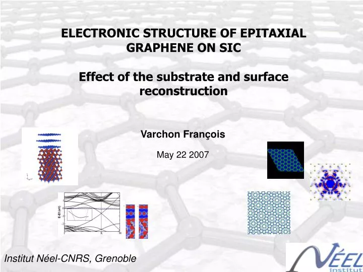
ELECTRONIC STRUCTURE OF EPITAXIAL GRAPHENE ON SIC Effect of the substrate and surface reconstruction. Varchon François. May 22 2007. Institut Néel-CNRS, Grenoble. Institut Néel Theory : Laurence Magaud ( ab initio, MCMF) Experiments :

E N D
ELECTRONIC STRUCTURE OF EPITAXIAL GRAPHENE ON SICEffect of the substrate and surface reconstruction Varchon François May 22 2007 Institut Néel-CNRS, Grenoble
Institut Néel • Theory : • Laurence Magaud (ab initio, MCMF) • Experiments : • Pierre Mallet and Jean-Yves Veuillen (STM, NANO) • Cécile Naud (transport, NANO) • Collaboration : • D.Mayou, V. Olevano, L. Levy, P. Darancet (IN) • B. Ngoc Nguyen, N. Wipf (IN) • C. Berger, E. Conrad and • W. de Heer (Gatech, Atlanta, USA) F. Varchon – Journées du graphène – 22 mai 2007
Graphene = 2D Cristal A atom B atom Electronic structure Cristal structure P.R. Wallace, Phys. Rev., 9 71, (1947) • Graphene = single carbon plane arranged on a honeycomb lattice • Linear band structure around K points : massless Dirac fermions • Physical properties : large phase coherence length (~μm at 4K), low electrical resistance, QHE at T ~ 300 K… F. Varchon – Journées du graphène – 22 mai 2007
Experimental realisation 1) Exfoliated graphene • A. Geim (2005) and P. Kim (2005): • K. S. Novoselov et al, Science 306, 666-669, (2004) • K. S. Novoselov et al, Nature 438, 197, (2005) • Y. Zhang et al, Nature 438, 201, (2005) A.Geim and K.S. Novoselov, Nature Materials 6, 183-191, (2007) 2) Epitaxial graphene • C. Berger and W. de Heer : • C.Berger et al., J.Phys. Chem.B 108, 19912 (2004) • C.Berger et al., Science 312, 1191, (2006) The graphene/graphite layers are produced by sublimating Si from SiC surface at sufficiently high temperature to graphitize the excess carbon Experiments on SiC (C-terminated): Several carbon layers stacked but evidence of graphene properties Influence of the substrate ? F. Varchon – Journées du graphène – 22 mai 2007
Plan 1. Effect of the substrate 2. Surface Reconstruction F. Varchon – Journées du graphène – 22 mai 2007
Plan Effect of the substrate F. Varchon – Journées du graphène – 22 mai 2007
C Si Epitaxial graphene on SiC 6H-SiC(0001) Si terminated 6H-SiC(0001) C terminated 2.5 Å F. Varchon – Journées du graphène – 22 mai 2007
Epitaxial graphene on SiC Carbon layers t Interface plane 6H-SiC(0001) Si terminated 6H-SiC(0001) C terminated C Si T 2.5 Å What is the geometry of the interface plane ? How does the interface between a graphene layer and its support affect its electronic properties ? F. Varchon – Journées du graphène – 22 mai 2007
Vienna ab initio simulation package (VASP) • DFT code developed by J. Hafner and G. Kresse (1989) • DFT calculations on different machines • highly optimized parallel code • Computational details: • 1. Periodic system : 9x9x1 grid in the Brillouin zone (K point is included) • Plane wave basis : Ecut-off=211 eV • Ultrasoft pseudopotentials (US-PP) • Exchange correlation energy functional : GGA-PW91 • Ionic relaxation : conjugate-gradient algorithm F. Varchon – Journées du graphène – 22 mai 2007
Interface SiC and graphene cells almost commensurate for6√3 x 6√3R30° cell. huge cell (>1000 atoms) Si C 1x1 √3 x √3 SiC(0001) surface+ 1 C layer Geometry for the interface layer Simplified geometry: √3 x √3 R30° -> corresponds to a 2X2 graphene cell -> 8% stretch of the graphene lattice parameter -> no qualitative effect on a free standing graphene electronic structure For the SiC interface layer : -> 2/3 are immediately below a C atom in the first carbon layer -> 1/3 has no atom above it Lonely atom F. Varchon – Journées du graphène – 22 mai 2007
Supercell Vaccum C SiC C Si H H • Electronic structure of a surface : • break the periodicity in the perpendicular axis of the surface • Supercell Supercell contains 59, 67 or 75 atoms : Carbon layers (1 ou 2 ou 3) on a honeycomb lattice with Bernal stacking + 8 SiC bi-layers in the 4H-SiC (0001) or (0001) geometry + 3 H atoms saturated the dangling bonds on the second side + vacuum 15 - 25 Å (to model the surface) F. Varchon – Journées du graphène – 22 mai 2007
Ionic relaxation Vaccum SiC (0001) (-Si) : d(SiC-1pl)= 2.0 Å d(1pl-2pl)= 3.8 Å d(2pl-3pl)= 3.9 Å C graphite DFT (2 - 5 Å) SiC SiC (0001) (-C) : d(SiC-1pl)= 1.66 Å1.65±0.005 Å d(1pl-2pl)= 3.9 Å 3.51±0.1 Å d(2pl-3pl)= 3.9 Å 3.370±0.005 Å C Si H H XRR E.Conrad Ionic relaxation : The first C layer has a strong interaction with SiC surface (Si-terminated or C-terminated) F. Varchon – Journées du graphène – 22 mai 2007
Dispersion curves for C-layers on SiC (C-terminated) 2 C layers 3 C layers 1 C layer 1 C layer : - no linear dispersion - not graphene = buffer layer 2 C layers : - linear dispersion = graphene - no doping = neutral graphene 3 C layers : - similar to the dispersion of a graphene bilayer. - no doping For all: state with a small dispersion at Efermi : Dangling bond (DB) state of the lonely atom F. Varchon – Journées du graphène – 22 mai 2007
Dispersion curves for C-layers on SiC (C-terminated) 2 C layers (C-deficient) Suppressed atom Si C 1x1 √3 x √3 • The lonely atom is suppressed (another possible interface geometry based on surface X-ray reflectivity data) : • - creating 3 dangling bonds at the interface • - n doping (Ef-Ed=0.4eV) • Electronic structure clearly depends on the geometry of the interface F. Varchon – Journées du graphène – 22 mai 2007
Dispersion curves for C-layers on SiC (Si-terminated) 1 C layer 2 C layers 3 C layers 1 C layer : - no linear dispersion - not graphene = buffer layer 2 C layers : - linear dispersion = graphene - graphene are doped (n type : 0.4 eV) 3 C layers : - 2 C layers are n doped - disymmetric graphene bilayer (gap) - one plane is less doped than the other one For all : small dispersion at Efermi : DB - interactions between DB and graphene - impact on transport properties ? F. Varchon – Journées du graphène – 22 mai 2007
Dispersion curves for C-layers on SiC (Si-terminated) 1 C layer 2 C layers Tight-binding, disymmetric bilayer: 3 C layers K.S. Novoselov et al., Nature Physics 2, 177-180, (2005) F. Varchon – Journées du graphène – 22 mai 2007
Dispersion curves for C-layers on SiC (Si-terminated) 1 C layer 2 C layers 3 C layers ARUPS, Ohta et al. Science 313,951 (2006) This is in agreement with ARPES measurements : F. Varchon – Journées du graphène – 22 mai 2007
Charge density SiC(0001) SiC(0001) C3 C2 • Evidence of the existence of a covalent bond between the buffer layer and SiC • - Si-C polar bond : n doping C1 C C C Si Si C SiC F.Varchon et al., cond-mat / 0702311 (submitted to PRL) F. Varchon – Journées du graphène – 22 mai 2007
Plan Surface reconstruction F. Varchon – Journées du graphène – 22 mai 2007
6 √3x 6 √3 R 30° C Si H • SiC and graphene cells almost commensurate for : • 6√3 x 6√3R30° for SiC • 13 x 13 for graphene • 6√3 x 6√3R30° Supercell: • 1216 atoms • 2 C layers (buffer layer + graphene) • 2 SiC bilayers • 1 H layer • vacuum (10 Å) F. Varchon – Journées du graphène – 22 mai 2007
6x6 reconstruction on SiC (-Si) STM image (12x12 nm2,0.2 V, 300 K) Ab initio (buffer layer) First graphene like layer 6x6 6x6 6√3x 6√3 R30° P.Mallet et al., cond-mat / 0702406 (submitted to PRL) • stress relaxation • apparent 6X6 reconstruction • Corrugation : - buffer layer : 1.2 Å (STM : 1-1.5 Å) • - graphene : 0.5 Å (STM : 0.2 – 0.4 Å) F. Varchon – Journées du graphène – 22 mai 2007
6X6 reconstruction on SiC (-C) Ab initio (buffer layer) 6x6 • stress relaxation • apparent 6x6 reconstruction • no STM image yet 6√3x 6√3 R30° F. Varchon – Journées du graphène – 22 mai 2007
CONCLUSION • Conclusion : • The first carbon layer on top of a SiC (-C) or (-Si) surface acts as a buffer layer « nanomesh » (existence of strong covalent bond buffer-SiC) • The buffer layer allows the next carbon planes to behave electronically like graphene/graphite layers • The carbon layers are n doped in the case of SiC (-Si) • Importance of the interface geometry (dangling bonds) • Evidence of 6x6 reconstruction observed by STM F. Varchon – Journées du graphène – 22 mai 2007
PERSPECTIVES • - more information on the interface geometry (electronic structure of the 6√3 x 6√3R30°) • - Transport properties in function of number of C layers, of stacking, interaction between planes… • - Influence of rotationnal disorder between two graphene layers : • - STM experiments: graphene on 6H-SiC (0001) F. Varchon – Journées du graphène – 22 mai 2007
Questions F. Varchon – Journées du graphène – 22 mai 2007
Graphene: candidat pour la nanoélectronique Ribbons CNT: - low electrical resistance - Choose between metalic/ semiconducting electronic structure for graphene ribbons: orientation and lateral size = CNT helicity armchair + 2D structure: - easy contact making - use of standard lithography technics - integration within devices zigzag K.Nakada et al PRL 54, 17954 (1996) F. Varchon – Journées du graphène – 22 mai 2007
Biplan de graphène F. Varchon – Journées du graphène – 22 mai 2007
Biplan de graphène S.Latil and L.Henrard, PRL 97, 036803 (2006) Latil A A B C C A A A B B C A A F. Varchon – Journées du graphène – 22 mai 2007
Théorie de la fonctionnelle de la densité (DFT) DFT = Méthode ab initio de résolution de l’équation de Schrödinger à N corps. • 1) Théorème de Hohenberg et Kohn (1964): • L’énergie E peut s’écrire sous la forme d’une fonctionnelle de la densité électronique n : E[n] • E[n] est minimisée par la densité de l’état fondamental n0 Conclusion d’HK: L’énergie totale d’un système de N électrons interagissant est donc fonctionnelle de la densité et la recherche de l’état fondamental peut être réalisée de manière itérative en se basant sur une loi variationnelle. F. Varchon – Journées du graphène – 22 mai 2007
Théorie de la fonctionnelle de la densité (DFT) • 2) Equations de Kohn-Sham (1965): • Système fictif de N électrons sans interaction (états de Kohn-Sham) de même densité électronique que les N électrons du système réel. • Résolution de N équations de Schrödinger « monoélectronique » • Minimisation de E[n] = résolution autocohérente des 3 équations interdépendantes de Kohn et Sham • DFT permet de calculer: • L’énergie interne d’un solide et la densité de l’état fondamental • Structure de bandes et densité d’état « approchées » (via les états de Kohn Sham) F. Varchon – Journées du graphène – 22 mai 2007
Scanning Tunneling Microscopy (STM) = Microscope à effet tunnel. • Topographie d’une surface d’un métal ou d’un semiconducteur à la résolution atomique. • Spectroscopie locale F. Varchon – Journées du graphène – 22 mai 2007
Nanomesh T=300K, Sample Bias -2.0V ! 6x6 30nm F. Varchon – Journées du graphène – 22 mai 2007
Graphene = 2D Cristal • Structures pour l’élément C: • 3D : diamond, graphite… • 2D : graphene • 1D : nanotubes • 0D : fullerenes A.Castro Neto, F.Guinea, N.M.Peres Physics World Nov 2006 • Graphène : • Cristal bidimensionnel d’atomes de carbone formé de cellules hexagonales. • Propriétés physiques remarquables : fermions de masse nulle, grande longueur de cohérence de phase (~µm à 4K°), QHE à T ambiante… • Intérêts pour les nanotechnologies : électronique cohérente, compatible avec les techniques de lithographie. F. Varchon – Journées du graphène – 22 mai 2007
Graphène = Cristal 2D atome A atome B Structure électronique Structure cristallographique • Pour chaque atome de C: • 3 orbitales hybrides sp2 • 1 orbitale pz Liaisons p etp*(liaisons fortes) : P.R. Wallace, Phys. Rev., 9 71, (1947) Graphène: Semi-Conducteur à Gap nul • 2 sous-réseaux d’atomes C • dA-B=1,418 Å • a=b=2,456 Å F. Varchon – Journées du graphène – 22 mai 2007
Structure électronique K K' M Brillouin zone Structure de bandes: DFT,VASP • Cônes de Dirac. • Dispersion linéaire aux points K de la première zone de Brillouin. • Les points K et K’ sont inéquivalents : • chiralité • (anti-) localisation • faible • Développement limité autour du point K : P.R. Wallace, Phys. Rev., 9 71, (1947) • Electrons : • Fermions de Dirac de masse nulle T.Ando, J. Phys. Soc. Jpn., 74 777-817, (2005) F. Varchon – Journées du graphène – 22 mai 2007
Graphène exfolié SiO2 Novoselov et al, Naturephysics 2006 2005 : mise en évidence expérimentale • Geim (2005) et P. Kim (2005): • K. S. Novoselov et al, Nature 438, 197, (2005) • Y. Zhang et al, Nature 438, 201, (2005) A.Geim and K.S. Novoselov, Nature Materials 6, 183-191, (2007) Le graphène est exfolié mécaniquement à partir du graphite et déposé sur un substrat de SiO2 Gaz d’électrons 2D Graphène Effet Hall semi-entier Signature du Graphène F. Varchon – Journées du graphène – 22 mai 2007
Graphène épitaxié T t SiC SiC C. Berger and W. de Heer (2006) : C.Berger et al., Science 312, 1191, (2006) Le graphène croît sous recuit de la surface du SiC, par désorption des atomes de Si et réarrangement des C Echantillon :Quelques plans de carbone (5-10ML) sur une surface SiC(0001) (terminée C) • Signature du graphène • Grande longueur de cohérence de phase (~μm à 4K) • Les propriétés de transport sont-elles dominées par 1 plan ? • Problème de couplage entre les plans Influence du substrat ? F. Varchon – Journées du graphène – 22 mai 2007