Download

1 / 81
1.16k likes | 1.94k Views
Traditional SOC Design Flow. Key Problem: Timing assumption during prelayout synthesis widely differs from the post layout reality. This happens because the interconnect delay dominates the overall propagation delay in DSM (Deep Sub-Micron) technologies.

E N D
Traditional SOC Design Flow • Key Problem: Timing assumption during prelayout synthesis widely differs from the post layout reality. • This happens because the interconnect delay dominates the overall propagation delay in DSM (Deep Sub-Micron) technologies. • As a result getting a timing closure becomes a challenge. Source: Advanced ASIC Chip Synthesis. 2nd Ed. Himanshu Bhatnagar. Kluwer Academic Publishers
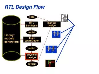
Set Design Constraints Develop HDL files Design Rule Constraints set_max_transition set_max_fanout set_max_capacitance Design Optimisation Constraints Create_clock set_clock_latency set_propagated_clock set_clock_uncertainty set_clock_transition set_input_delay set_output_delay set_max_area Specify Libraries Library Objects link_library target_library symbol_library synthetic_library Read Design analyze elaborate read_file Select Compile Strategy Top Down Bottom Up Define Design Environment Optimize the Design Set_operating_conditions Set_wire_load_model Set_drive Set_driving_cell Set_load Set_fanout_load Set_min_library Compile Analyze and Resolve Design Problems Check_design Report_area Report_constraint Report_timing Save the Design database write
Design Compiler Setup Files • .synopsys_dc.setup • Library paths • Company wide, project wide design environment related variables and commands • UNIX variables • Three files at three locations. All three are read in the following order • Synopsys root - $SYNOPSYS/admin/setup • Affects all users. Only system adminstrator can modify this. In small startups with only single ASIC project, this serves as the place to enforce project wide discipline. • Home Directory • Content affects all DC activities. Project wide enforcement could happen at these level if the designer is involved in a single project (less likely). • Working Directory • Affects the current invocation of DC. If a person is working on more than one Synopsys projects (more likely), then the project wide enforcement should happen at this level. One working directory for each project. • Repeated commands are overridden
Technology Library Created by ASIC vendor in Synopsys format – which is now an open standard. Cells are defined by their names, function, timing, net delay, parasitic information, units for time, resistance, capacitance etc. Target Library a technology library that Design Compiler maps to during optimization. Link Library The technology library that contains the definition of the cells used in the mapped design. In principle should be the same as target_library unless a technology translation is being performed. Libraries & Search Path • Symbol Library Definition of graphics symbols. Cells in Symbol Library must match • DesignWare Library A DesignWare component library is a collection of reusable circuit-design building blocks that are tightly integrated into the Synopsys synthesis environment. • GTECH Library The GTECH library is the Synopsys generic technology library. It is technology-independent and included with Design Compiler software. GTECH parts are Synopsys unmapped representations of Boolean functions (library cell placeholders). GTECH instantiation allows for a technology-independent HDL description and the accuracy of instantiation. • Search_path If the library variables only specify file names, search_path is used to locate libraries. By default points to current working directory and $SYNOPSYS/libraries/syn
Synopsys Design Objects • Design A circuit that performs one or more logical functions • Cell An instance of a design or library primitive within a design • Reference The name of the original design that a cell instance points to • Port The input or output of a design • Pin The input or output of a cell • Net A wire that connects ports to ports or ports to pins • Clock A timing reference object to describe a waveform for timing analysis
Reading Assignment Read about these commands from Synopsys Documentation Find and Filter Read / Analyze / Elaborate Compile Report_timing Also read about what are Attributes and Variables
Outline of this course module Synopsys Design Environment Essentials CMOS essentials for logic synthesis Constraint Classification Load and Drive Constraints Clocking constraints Operating Conditions Constraints Static Timing Analysis Chip Level Timing and Multiple Clock Domains
MOSFET Transistor Source: MIT. Course 6.375. Lecture L06. 2006
Key qualitative Characteristics of MOSFET transistors Source: MIT. Course 6.375. Lecture L06. 2006
RC Model of an inverter Source: MIT. Course 6.375. Lecture L06. 2006
Wires Source: MIT. Course 6.375. Lecture L06. 2006
Distributed RC wire model This is also known as Elmore Delay model Source: MIT. Course 6.375. Lecture L06. 2006
Manual insertion of Repeaters Source: MIT. Course 6.375. Lecture L06. 2006
Lumped RC wire model Source: MIT. Course 6.375. Lecture L06. 2006
Estimate the rise time Source: MIT. Course 6.375. Lecture L06. 2006
Width of transistor is found by multiplying the scaling factor (16/8/2/1) with the minimum width of transistor which is 0.5 mm. Multiply Cg,N/Cg,P/Cd,N/Cd,P with the width of the transistor to get the drain/gate capacitances for P and N transistors. Wider transistor more capacitance Divide Reff,N/Reff,P with the width of the transistor to get the Resistance for the N and P transistors. Wider Transistor Less resistance The factor 2.2 comes from 90% Vdd swing loge(0.9Vdd/ 0.1Vdd) The sheet resistance (0.07) is for unit square. Since the wire width is 0,25mm. resistance for 1 mm X 0.25 mm wire is 0.07/0.25. This factor is multiplied by the length 250 mm The wire capacitance is made up of two parts: Bottom (area) capacitance found using 250 X 0.25 (area) X CA,M2. Side capacitance is found by multiplying length 250 XCL,M32 Source: MIT. Course 6.375. Lecture L06. 2006
Constraints • Optimisation Constraints • Performance – clock • Area • Power • Technology, Operating and Manufacturing Constraints • Max rise time, max capacitance • Operating Conditions – • Vdd, Temperature • Drive current, Load • Process Variations • Fast corner, Slow corner • Physical Design • Antenna rules
Generic Synthesis Flow Design Create a solution Technology, Operating & Manufacturing Constraints Optimisation Constraints Evaluate the solution Analysis Constraints Met
Static Timing Analysis (STA) • Exhaustively verifies that • the timing constraints (clock) are met for a design • for given technology (Standard Cell Library) and • a set of specified operating conditions • Limitations of the alternative – Simulation • Not Exhaustive • Accuracy • RTL • Gate Level • SDF back annotation • Dependent on STA • Circuit Level SPICE simulation are impractical • Time (STA also takes time, but is bounded) PROCESS (clk) BEGIN IF rising_edge (clk) THEN s <= a * b; END IF; END
Timing Models - Accuracy • Untimed • Transaction Level - SystemC • Multiple Cycles • Bus Transactions, Transmit/Receive, Encode/Decode • Cycle Accurate – RTL • What happens in each clock cycle is accurately known • Gate Level – Event Driven • Physical details of computation, storage and interconnect operations known • Delay in wire is not known • Clock is ideal • Layout Level • Delay in wire known • Clock is real • Relative position of standard cell is known
Delay Parameters – Intrinsic Delay & Slew A=1 Z B Vdd B Z Vdd 0.7Vdd R z 0.5Vdd y Q 0.3Vdd P x t1 t1 t2 t2
Path Delay Calculation • The intrinsic delays and the slews are characterised using SPICE simulation by sweeping many parameters that affects the Intrinsic delay and Slew • All the paths are exhaustively covered Library and Design Environment Conditions for Analysis A Delay Computation Through Wire Delay Computation Through Gate Delay and Slew At Gate Output B D Delay and Slew At Next Gate Input C
Paths & Path Groups • Paths • Start point: Input ports or clock pins of sequential devices and • End point: Output ports or Data input pins of sequential devices. • Path groups • Paths are organised in groups identified by clocks controlling their endpoints.
Timing Arcs • positive unate timing arc: • Combines rise delays with rise delays, and fall delays with fall delays. An example is an AND gate cell delay or an interconnect (net) delay. • negative unate timing arc: • Combines incoming rise delays with local fall delays, and incoming fall delays with local rise delays. An example is a NAND gate. • nonunate timing arc: • Combines local delay with the worst-case incoming delay value. Nonunate timing arcs are present in logic functions whose output value change cannot be predicted by the direction of the change on the input value. An example is an XOR gate. • Accuracy of estimates is critical • Intrinsic Delays are accurate after logic synthesis • Slew and Net Delays are estimated and known accurately only after physical synthesis
Factors Affecting Delay and Slew Discrete Factors: Geometry & Dimension Specific Path Transition Direction Related Pin P1 P2 Z A N1 4 Input NAND gate B N2
Factors Affecting Delay and Slew • Load on the Gate • Load of all the inputs that this output has to drive • Load of the interconnect wires • Tri-stated wires • Input Slew • Transition time at the previous gate • The interconnect • Primary input – drive strength, driver cell
Constraints • Technology Constraints • Max Transition • Max Fanout • Max Capacitance • Min Capacitance • Design Constraints • Set Load • Set Drive (inverse of resistance)
5 Z1 A Z2 A Z3 set_driving_cell set_load or set_drive Technology Constraint; Cannot be relaxed Design Constraint • If drive or driving cell is not specified, the synthesis tool assumes infinite drive strength • If load is not specified, the synthesis tool assumes zero load
Interpolation and Extrapolation Piece Wise Linear Model Load D12 D22 L2 L D2 D1 D L1 D11 D21 S S1 S2 Slew
worst worst worst Delay nominal Delay nominal Delay nominal best best best Process Temperature Voltage Process, Voltage, Temperature (PVT) Variation & Operating Conditions Operating Conditions Name Library Process Temp Volt Interconnect Model WCCOM my_lib 1.50 70 1.1 worst_case_tree WCIND my_lib 1.50 80 1.1 worst_case_tree WCMIL my_lib 1.50 125 1.0 worst_case_tree BCCOM my_lib 1.50 0 1.2 best_case_tree BCIND my_lib 1.50 -40 1.2 best_case_tree BCMIL my_lib 1.50 -55 1.3 best_case_tree
PVT Variation: An Example Consider a minimum size NMOS device in a 1.2 mm CMOS process. VGS =VDS = 5V The nominal saturation current for the device size W = 1.8 mm, Leff = 0,9 um Now consider the variation in the following parameters: • 25 % variation in Threshold voltage – Vt • 10 % variation in transconductancek’n mainly due to variation in oxide thickness. • ±0.15mm (about 10 %) variation in W and L. Variations in W and L are uncorrelated as they are • ±0.5V (10%) variation in power supply voltage Speed of device is proportional to the drain current and can thus result in variation of the speed of the circuit.
Derating Libraries are characterized for various operating conditions Further characterisation is done to see how the delay model responds to change in process, voltage and temperature. This is done by holding two parameters constant and sweeping the third. This yields derating factors for Process, Voltage and Temperature
Sequential Arcs Timing relationship between two input pins two consecutive events on the same input pin Pulse Width Setup Hold Recovery Removal
Pulse Width Width of High and low phases of clocks Width of Active level of asynchronous inputs like reset Not met. Reset may have no effect rst_n Pulse Width Requirement
Setup Data should be stable setup time before the arrival of clock edge. What happens if the setup time is violated ? Not met. New data may not get latched clk data Setup Requirement
Hold Data should be stable hold time after the arrival of clock edge. What happens if the Hold time is violated ? Not met. Old data may not get latched clk data Hold Requirement
Recovery and Removal Minimum time between de-assertion of an asynchronous control signal and the next active clock edge Minimum time between an active clock edge that an asynchronous control signal should remain asserted rst_n Not met. clk may not have effect Not met. clk may override rst_n clk clk rst_n Recovery Requirement Removal Requirement Can be formulated as a setup check Can be formulated as a hold check
What is the reason for setup and hold a Vin2 = Vout1 Vin1 Vout1 Vin2, Vout1 c c Vin2 Vout2 b Vin1 = Vout2 Vin1, Vout2 a b
Transistor Level Schematic of a D-Flophttp://www.edn.com/design/analog/4371393/Understanding-the-basics-of-setup-and-hold-time
Working of the D-Flop work at Transistor Level http://www.edn.com/design/analog/4371393/Understanding-the-basics-of-setup-and-hold-time
Setup and Hold Time at Circuit Level The time it takes data D to reach node Z is called the setup time. The time it takes data D to reach node W is called the hold time. http://www.edn.com/design/analog/4371393/Understanding-the-basics-of-setup-and-hold-time